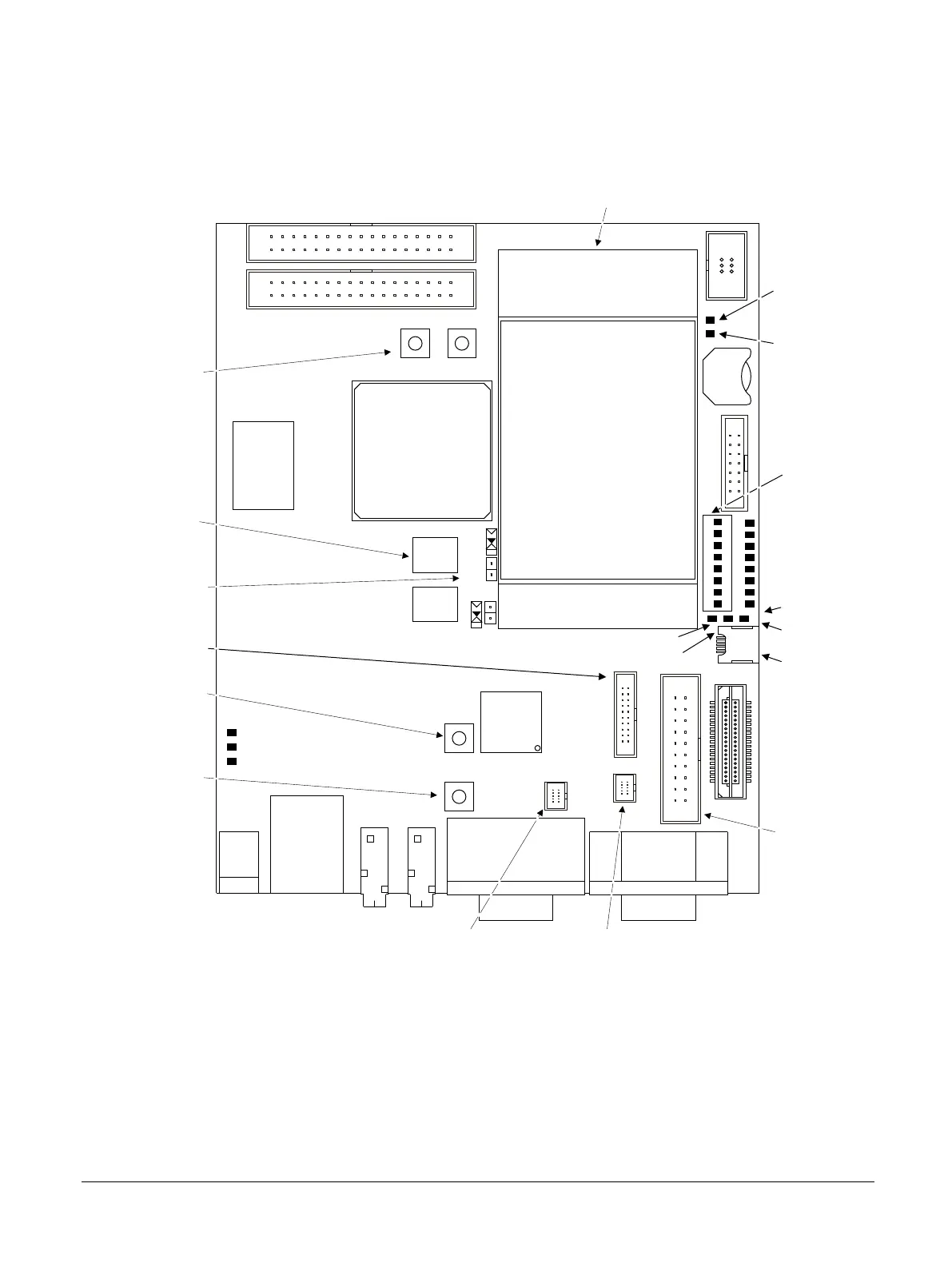
1.4 Location of components on the MPS2+ FPGA Prototyping Board
The following figure shows the upper face of the MPS2+ FPGA Prototyping Board.
Expansion
connector
EXP2
Expansion
connector
EXP1
LCD display panel
2MB ZBT
SSRAM
12V DC
power jack
RJ45
Ethernet
connector
Out
VGA
General
purpose
UART
Stereo line
audio
JTAG 14
connector
JTAG 20
connector
MICTOR 38
connector
CoreSight 20
connector
CoreSight 10
connector
Reserved
MCC
PSRAM
8MB
ON/OFF
soft RESET
push button
Hardware
RESET
push button
MCC
user
LEDs
FPGA user push
buttons
PB0PB1
SPI
header
In
Altera Cyclone 5CEA9
FPGA
MCC user
switches
Clock
connection
headers and
slide switches
J22
J23
J18
J19
Ethernet
activity
LEDs
DPLX
LINK
100Mbs
USB 2.0
configuration
port
FPGA
user
LED 1
1
8
7
6
5
4
3
2
HDD
PWR
DONE
System
LEDs
1
8
7
6
5
4
3
2
FPGA
user
LED 0
3V battery
Figure 1-3 Upper face of the MPS2+ FPGA Prototyping Board
The following figure shows the lower face of the MPS2+ FPGA Prototyping Board.
1 Introduction
1.4 Location of components on the MPS2+ FPGA Prototyping Board
100112_0200_09_en Copyright © 2013–2016, 2018–2020 Arm Limited or its affiliates. All
rights reserved.
1-19
Non-Confidential