4.4 SCC register descriptions
This section describes the SCC registers in the FPGAs on the MPS2 and MPS2+ FPGA Prototyping
Boards.
This section contains the following subsections:
• 4.4.1 Overview of SCC registers on page 4-63.
• 4.4.2 SCC_CFG0 Register on page 4-63.
• 4.4.3 SCC_CFG1 Register on page 4-64.
• 4.4.4 SCC_CFG3 Register on page 4-64.
• 4.4.5 SCC_CFG4 Register on page 4-65.
• 4.4.6 SCC_DLL Register on page 4-66.
• 4.4.7 SCC_AID Register on page 4-67.
• 4.4.8 SCC_ID Register on page 4-68.
4.4.1 Overview of SCC registers
The MCC on the MPS2 or MPS2+ FPGA Prototyping Board writes to the SCC registers in the FPGA at
powerup with the values that the configuration board file defines.
During runtime, the MCC polls the LED and switch values to ensure that they match the SCC_CFG1 and
SCC_CFG2 register values. The MCC updates the LEDs to match the SCC_CFG1 register values and
updates the SCC_CFG2 register to match the user switches.
The SCC_CFG3 register contains board revision information.
The MCC reads the SYS_DLL, SCC_AID and SCC_ID registers to determine whether the PLLs in the
FPGA are locked and to determine the loaded FPGA image.
4.4.2 SCC_CFG0 Register
The SCC_CFG0 Register characteristics are:
Purpose
Remaps block RAM to ZBT.
Usage constraints
There are no usage constraints.
Configurations
Available in all MPS2 and MPS2+ configurations.
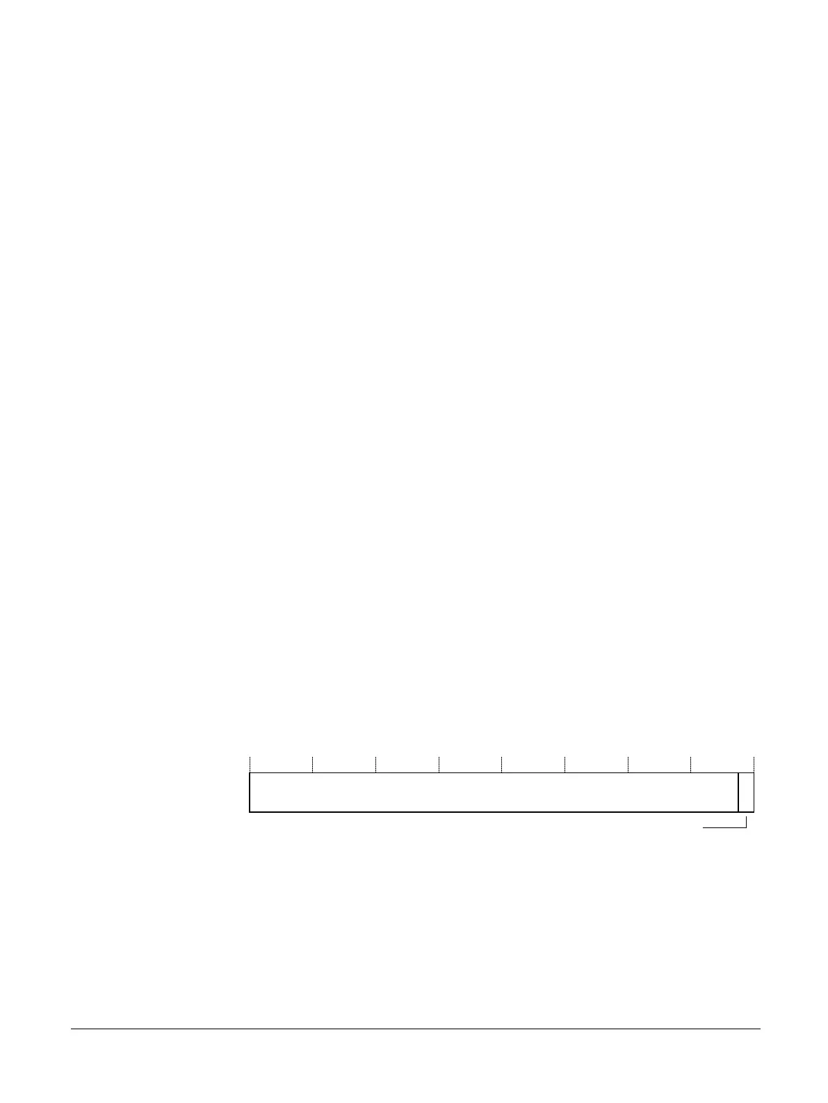
The following figure shows the bit assignments.
31
0
Reserved
Remap block RAM to ZBT
1
0
Figure 4-1 SCC_CFG0 Register bit assignments
The following table shows the bit assignments.
4 Programmers Model
4.4 SCC register descriptions
100112_0200_09_en Copyright © 2013–2016, 2018–2020 Arm Limited or its affiliates. All
rights reserved.
4-63
Non-Confidential