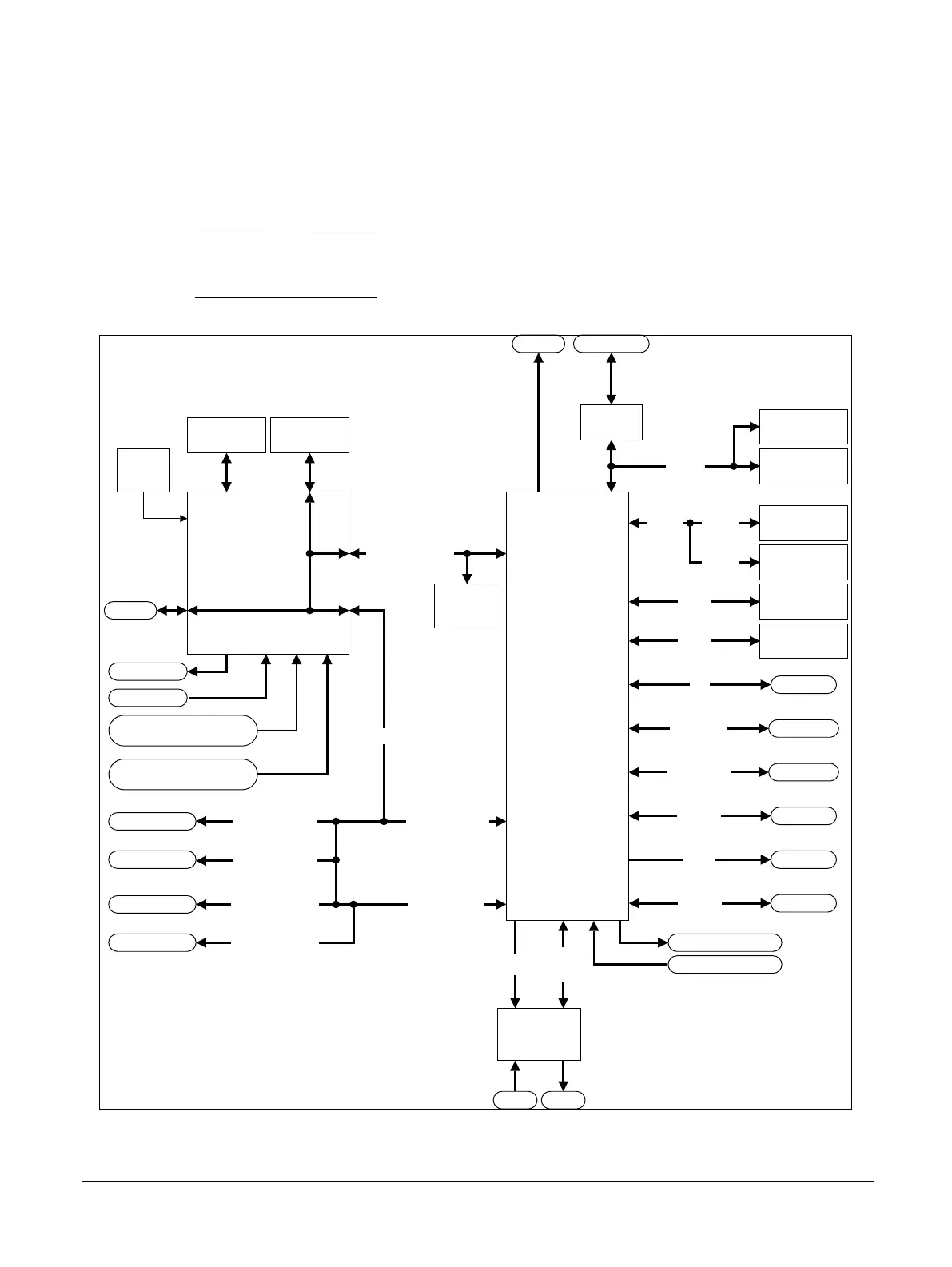
2.1 Overview of the MPS2 and MPS2+ hardware
The hardware infrastructure supports Arm M-class processor evaluation and development, system
expansion, and debug interfaces.
The following figure shows the high-level hardware infrastructure.
Note
The image that the configuration systems loads into the FPGA at powerup defines the functionality of the
MPS2 and MPS2+ FPGA Prototyping Boards.
MPS2/MPS2+ FPGA Prototyping Board
Clock
generators
FPGA
ZBT SSRAM 1
2MB
32-bit
32-bit
User push buttons
LEDs
microSD card
(USBMSD)
Configuration
EEPROM
JTAG 14
UART
VGA
ETHERNET
EXP[51:26]
USB 2.0
ZBT SSRAM 2
2MB
PSRAM 1
8MB
ZBT SSRAM 3
2MB
Expansion
CLCD
MCC
MAC/PHY
DIP switches
LEDs
EXP[25:0]
Stereo audio
codec
Audio Audio
CLCD
F-JTAG
CoreSight 10
CoreSight 20
MICTOR 38
P-JTAG/SWD
16-bit Trace
SCC
VGA
Configuration
ON/OFF/Soft RESET
push button
Hardware RESET push
button
P-JTAG/SWD
4-bit Trace
4-bit Trace
16-bit Trace
I
2
C
I
2
S
audio
SPI
SPI
Expansion
ZBT SSRAM 1
2MB
64-bit
PSRAM 0
8MB
16-bit
32-bit
32-bit
JTAG 20
P-JTAG/SWDP-JTAG/SWD
P-JTAG/SWD
CMSIS-DAP
3V
battery
Real Time Clock
Figure 2-1 Board hardware infrastructure
2 Hardware Description
2.1 Overview of the MPS2 and MPS2+ hardware
100112_0200_09_en Copyright © 2013–2016, 2018–2020 Arm Limited or its affiliates. All
rights reserved.
2-22
Non-Confidential