5.7 VGA connector
The MPS2 and MPS2+ FPGA Prototyping Boards provide one VGA connector that supports VGA and
CLCD output.
The VGA connector connects to the VGA controller which connects to general‑purpose pins on the
FPGA. The availability of VGA or CLCD depends on the design which you implement in the FPGA.
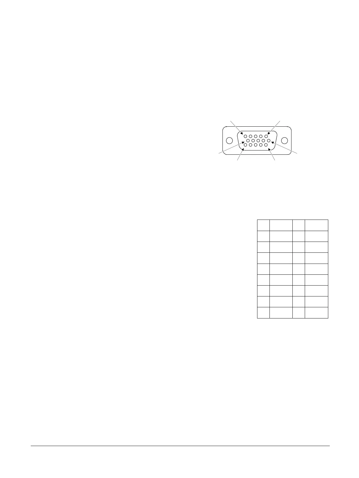
The following figure shows the VGA connector.
Pin 1
Pin 5
Pin 11Pin 15
Pin 6Pin 10
Figure 5-11 VGA connector
The following table shows the pin mapping for the VGA connector J10.
Table 5-12 VGA connector, J10, signal list
Pin Signal Pin Signal
1 RED 2 GREEN
3 BLUE 4 NC
5 GND 6 GND
7 GND 8 GND
9 NC 10 GND
11 NC 12 NC
13 HSYNC 14 VSYNC
15 NC
Related information
2.8 VGA and CLCD interfaces on page 2-32
1.3 Location of components on the MPS2 FPGA Prototyping Board on page 1-17
1.4 Location of components on the MPS2+ FPGA Prototyping Board on page 1-19
5 Signal Descriptions
5.7 VGA connector
100112_0200_09_en Copyright © 2013–2016, 2018–2020 Arm Limited or its affiliates. All
rights reserved.
5-86
Non-Confidential