5.3 CLCD connector
The MPS2 and MPS2+ FPGA Prototyping Boards provide a female IDC connector that supports CLCD.
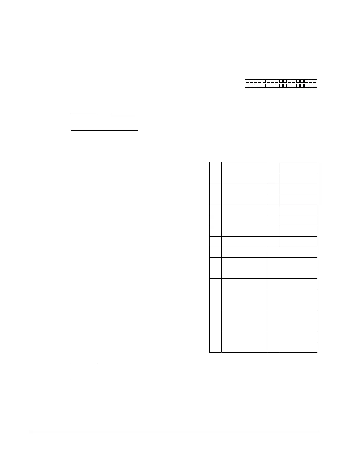
The following figure shows the CLCD connector.
1
2
33
34
Figure 5-7 CLCD connector
Note
A mark on the board indicates pin 1.
The following table shows the pin mapping for the CLCD connector J9.
Table 5-8 CLCD connector, J9, signal list
Pin Signal Pin Signal
1 CLCD_T_SCL 2 CLCD_T_SDA
3 CLCD_CS 4 CLCD_RS
5 CLCD_WR_SCL 6 CLCD_RD
7 CLCD_RESET 8 CLCD_PD1
9 CLCD_PD2 10 CLCD_PD3
11 CLCD_PD4 12 CLCD_PD5
13 NC 14 NC
15 NC 16 NC
17 NC 18 NC
19 NC 20 NC
21 NC 22 NC
23 NC 24 GND
25 CLCD_BL_CTRL 26 3V
27 3V 28 GND
29 GND 30 3V
31 CLCD_SDO 32 CLCD_SDI
33 CLCD_T_CS 34 CLCD_T_SCK
Note
Pins 1, 2, 5, 31, and 32 have 10k pullup resistors to 3V.
Related information
2.8 VGA and CLCD interfaces on page 2-32
1.3 Location of components on the MPS2 FPGA Prototyping Board on page 1-17
1.4 Location of components on the MPS2+ FPGA Prototyping Board on page 1-19
5 Signal Descriptions
5.3 CLCD connector
100112_0200_09_en Copyright © 2013–2016, 2018–2020 Arm Limited or its affiliates. All
rights reserved.
5-82
Non-Confidential