2.13 MCC FPGA serial interface
This section describes the Serial Configuration Controller (SCC) between the MCC and the FPGA.
This section contains the following subsections:
• 2.13.1 Serial Configuration Controller (SCC) on page 2-39.
• 2.13.2 SCC READ and WRITE operations on page 2-40.
• 2.13.3 SCC READ and WRITE timings on page 2-40.
2.13.1 Serial Configuration Controller (SCC)
The MCC uses a serial communication channel to receive from and transmit information to the FPGA on
the board. You must implement a Serial Configuration Controller (SCC) in the FPGA.
Overview of MCC-SCC interface
The SCC interface operates at 0.5MHz. The serial interface is similar to a memory-mapped peripheral
because it has an address and data phase.
The nCFGRST output from the MCC loads the default configuration settings into the FPGA.
CFGLOAD determines when WRITE DATA is complete, or when the system expects READ DATA to
be ready. The MCC provides the SCC clock. CFGWnR changes depending on the access type. The SCC
operates a 12-bit address and 32-bit data phase.
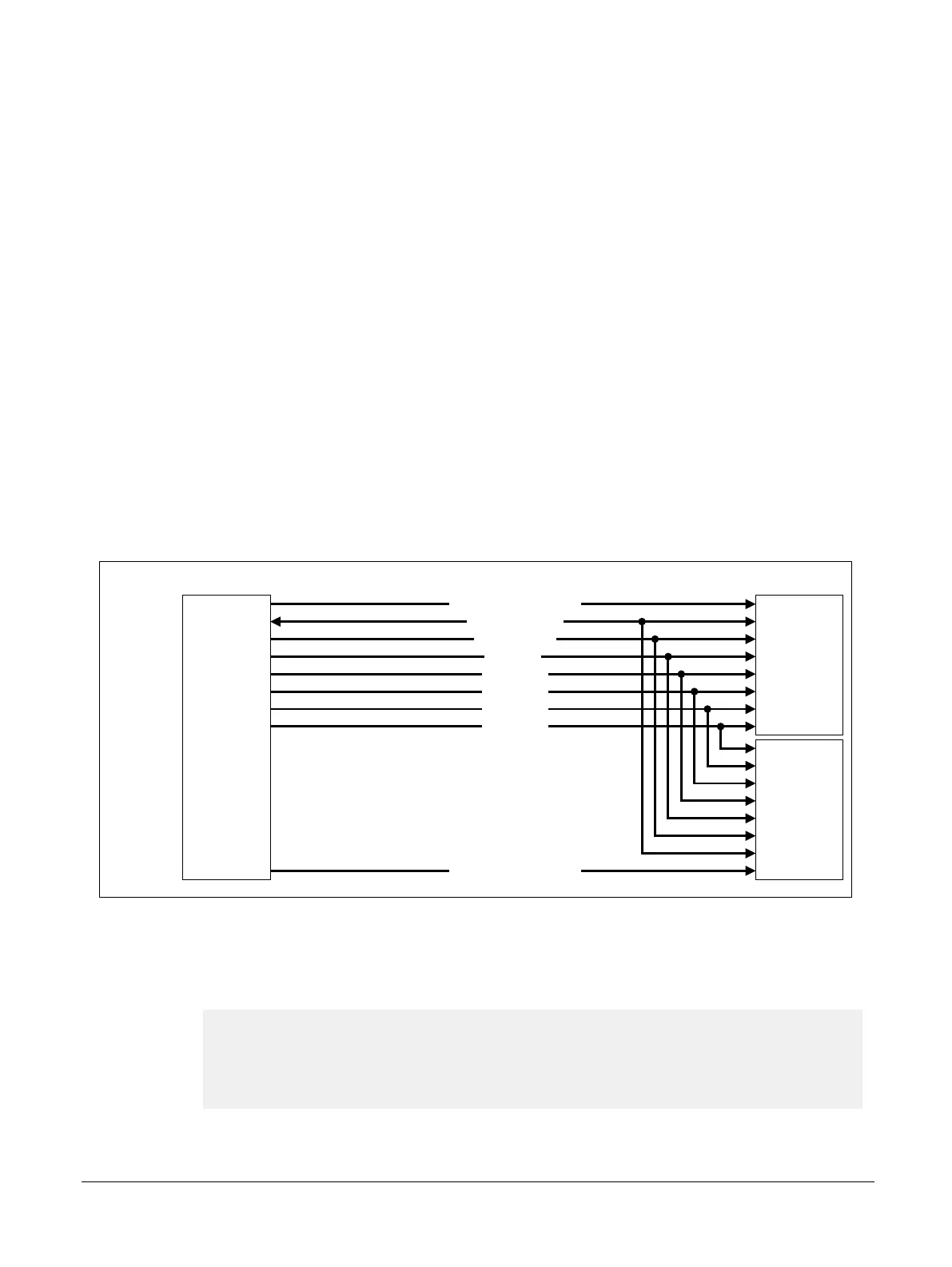
The following figure shows the MCC-SCC interface.
MPS2/MPS2+ FPGA Prototyping Board
FPGA
PSRAM 8MB
SMB_nZZ
SMB_nOE
SMB_nWE
SMB_A[21:0]
SMB_nUB
SMB_nLB
SMB_DQ[15:0]
SMB_PSRAM_nCE[1]
PSRAM 8MB
SMB_PSRAM_nCE[0]
Figure 2-14 MCC-FPGA serial interface
FPGA pin assignments to implement an MCC-SCC interface
If you implement an SCC interface, you must make the following pin assignments in the FPGA:
assign CFGCLK = CLCD_PDH[13];
assign nCFGRST = CLCD_PDH[14];
assign CFGLOAD = CLCD_PDH[15];
assign CFGWnR = CLCD_PDH[16];
assign CFGDATAIN = CLCD_PHD[17];
assign CLCD_PDH[12] = CFGDATAOUT;
2 Hardware Description
2.13 MCC FPGA serial interface
100112_0200_09_en Copyright © 2013–2016, 2018–2020 Arm Limited or its affiliates. All
rights reserved.
2-39
Non-Confidential