2.8 VGA and CLCD interfaces
The MPS2 and MPS2+ FPGA Prototyping Boards support VGA and CLCD video output.
Overview of the VGA interface
The VGA interface consists of a VGA controller in the FPGA, a passive resistor network, and an output
VGA port. The VGA output has 4 bits per channel color depth.
Overview of the CLCD interface
The CLCD interface consists of an SPI bus that is connected between the FPGA and a CLCD connector
and an LCD touch screen.
The LCD Thin Film Technology (TFT) display panel is fitted to the CLCD connector and has 320x240
pixel resolution. The panel includes a 4-wire resistive touch screen and an STEMPE811 touch screen
controller that is connected to the FPGA over an I
2
C bus.
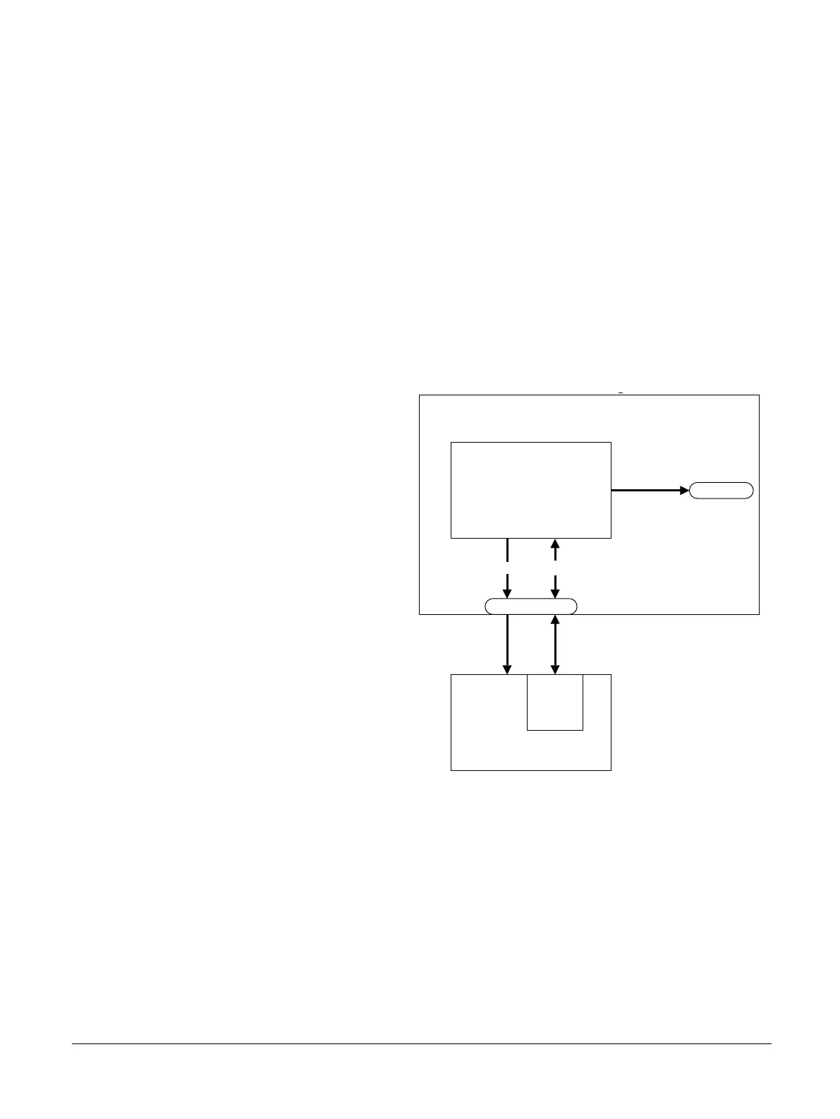
The following figure shows the board VGA and CLCD interfaces.
MPS2/MPS2+ FPGA Prototyping Board
FPGA
VGA
CLCD
SPI
VGA
LCD panel
I
2
C
Touch
Screen
controller
Figure 2-8 VGA and CLCD interfaces.
LCD panel
The LCD panel is configured for SPI graphics and I
2
C touch-screen.
Related information
1.3 Location of components on the MPS2 FPGA Prototyping Board on page 1-17
1.4 Location of components on the MPS2+ FPGA Prototyping Board on page 1-19
5.3 CLCD connector on page 5-82
5.7 VGA connector on page 5-86
2 Hardware Description
2.8 VGA and CLCD interfaces
100112_0200_09_en Copyright © 2013–2016, 2018–2020 Arm Limited or its affiliates. All
rights reserved.
2-32
Non-Confidential