2.11 User switches and user LEDs
The MPS2 and MPS2+ FPGA Prototyping Boards provide a user interface that consists of user LEDs
and user switches that connect to the FPGA and MCC. The FPGA image and application software define
their meaning.
The board provides the following LEDs and switches:
• Two LEDs and two push buttons that connect directly to the FPGA:
— The board labels the LEDs as USERLED0 and USERLED1.
— The board labels the push buttons as PB0 and PB1.
• Eight LEDs and an 8-way DIP switch that connect to the MCC.
You can write the values from these LEDs and switches to system registers inside the FPGA using a
serial SCC interface.
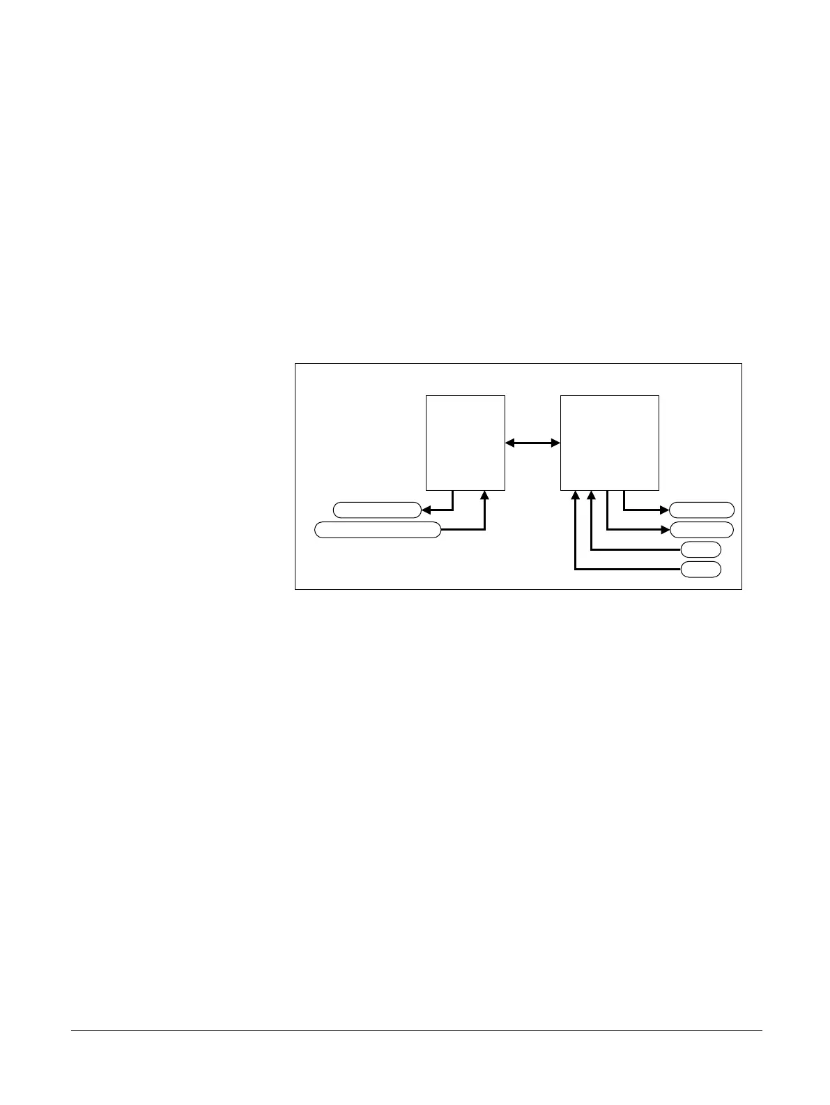
The following diagram shows the user switches and LEDs that form the FPGA and MCC user interface.
MPS2/MPS2+ FPGA Prototyping Board
PB0
USERLED0
MCC FPGA
SCC
PB1
USERLED1User DIP switches 1-8
User LEDs 1-8
Figure 2-11 FPGA and MCC user interface
Related information
1.3 Location of components on the MPS2 FPGA Prototyping Board on page 1-17
1.4 Location of components on the MPS2+ FPGA Prototyping Board on page 1-19
4.4.3 SCC_CFG1 Register on page 4-64
4.4.4 SCC_CFG3 Register on page 4-64
2.13 MCC FPGA serial interface on page 2-39
2 Hardware Description
2.11 User switches and user LEDs
100112_0200_09_en Copyright © 2013–2016, 2018–2020 Arm Limited or its affiliates. All
rights reserved.
2-35
Non-Confidential