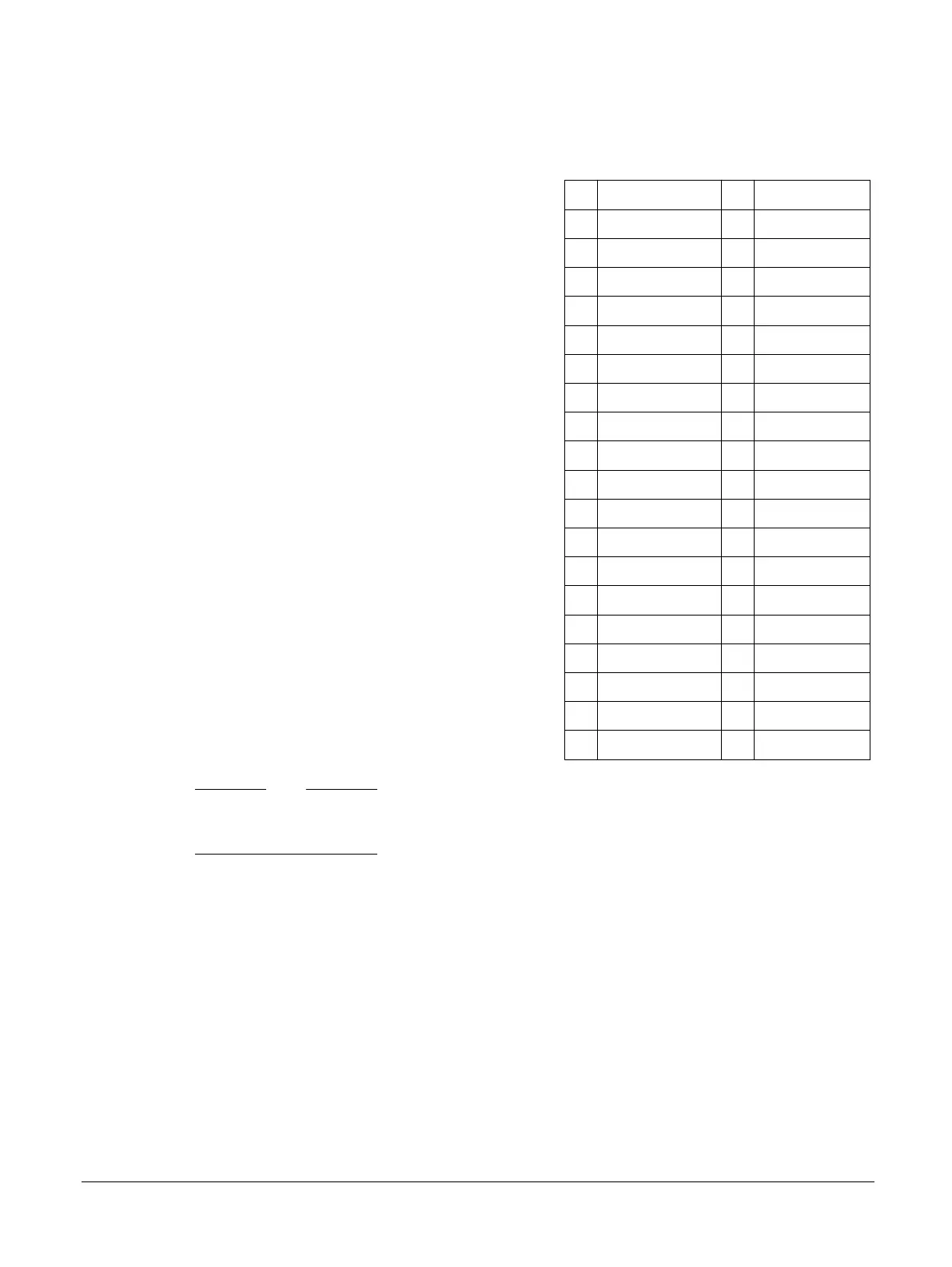
The following table shows the pin mapping for each P-JTAG, SWD, and 16-bit Trace signal on the
MICTOR 38 connector J6.
Table 5-5 MICTOR 38 connector, J6, signal list
Pin Signal Pin Signal
1 NC 2 NC
3 NC 4 NC
5 GND 6 TRACECLK
7 GND 8 GND
9 NC/nSRST 10 GND
11 TDO/SWO 12 3V reference
13 RTCK 14 3V0_OUT
15 TCK/SWCLK 16 TRACEDATA[7]
17 TMS/SWDIO 18 TRACEDATA[6]
19 TDI 20 TRACEDATA[5]
21 nTRST 22 TRACEDATA[4]
23 TRACEDAT[15] 24 TRACEDATA[3]
25 TRACEDAT[14] 26 TRACEDAT[2]
27 TRACEDATA[13] 28 TRACEDATA[1]
29 TRACEDATA[12] 30 GND
31 TRACEDATA[11] 32 GNDDETECT
33 TRACEDATA[10] 34 3V reference
35 TRACEDATA[9] 36 TRACECTL
37 TRACEDATA[8] 38 TRACEDATA[0]
Note
• Pins 9, 11, 17, 19 and 21 have pullup resistors to 3V.
• Pin 15 has a pulldown resistor to GND.
Related information
2.15.3 P-JTAG on page 2-45
2.15.5 16-bit Trace on page 2-45
2.15.6 Serial Wire Debug on page 2-45
1.3 Location of components on the MPS2 FPGA Prototyping Board on page 1-17
1.4 Location of components on the MPS2+ FPGA Prototyping Board on page 1-19
5 Signal Descriptions
5.1 Debug connectors
100112_0200_09_en Copyright © 2013–2016, 2018–2020 Arm Limited or its affiliates. All
rights reserved.
5-79
Non-Confidential