2/24/2008 9T6WP
BCM7405 Preliminary Hardware Data Module
Timing and AC Characteristics 06/29/07
Broadcom Corporation
Page 1-150 Data Transport Input Timing Document 7405-1HDM00-R
DATA TRANSPORT INPUT TIMING
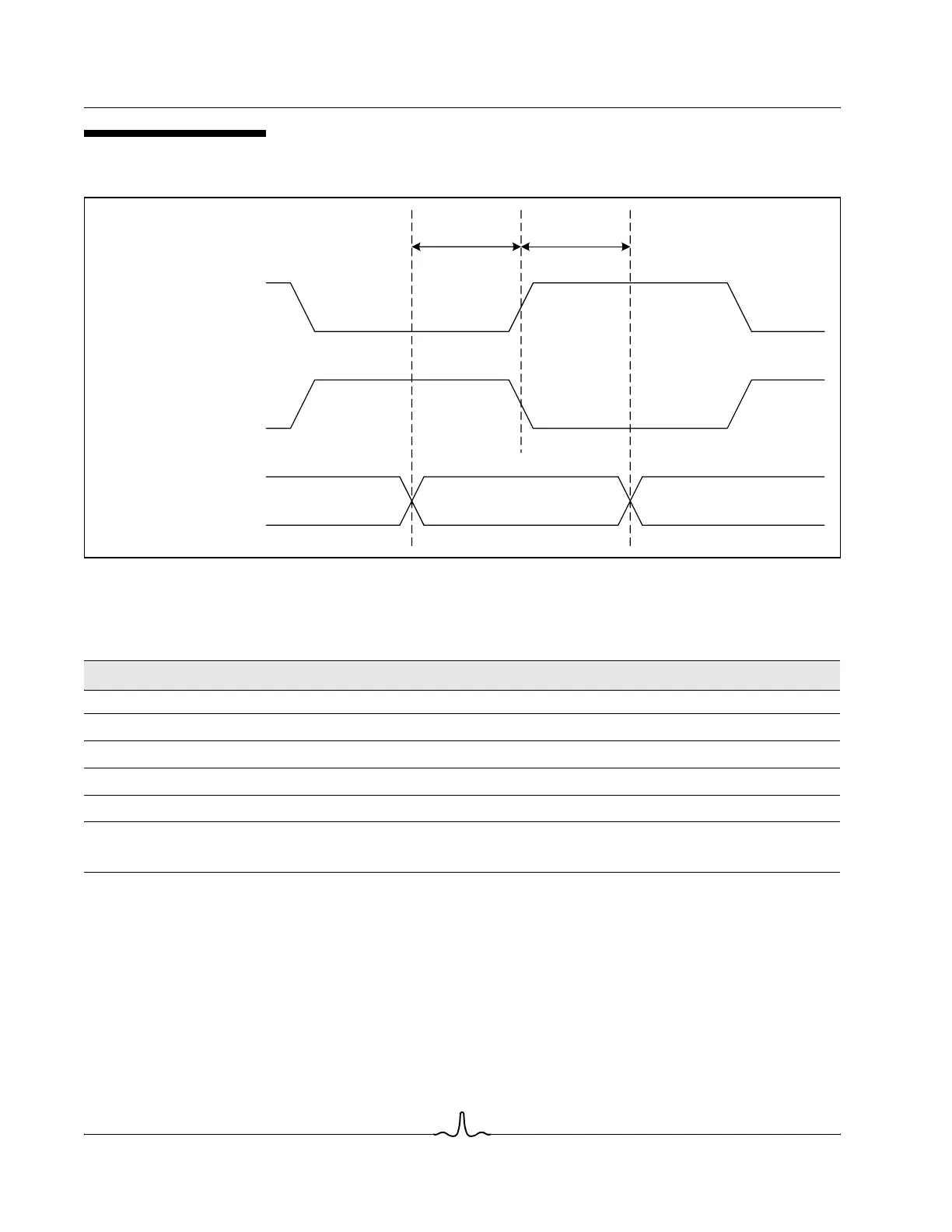
Figure 1-35: Data Transport Input Band Timing
Table 1-21: Data Transport Input Band Timing Parameters
Description Symbol Min. Max. Units
IB_CLK frequency Fs – 100 MHz
IB_CLK rise time
1
Trise–2ns
IB_CLK fall time
1
Tfall–2ns
IB_DATA, IB_SYNC Setup Time to IB_CLK active edge (rising or falling)
2
Tsu4–ns
IB_DATA, IB_SYNC Hold Time from IB_CLK active edge (rising or falling)
2
Thd4–ns
1
Rise and Fall time specs are measured from the 10% and 90% VDD levels.
2
The active clock edge for IB_CLK is programmable to either the rising or falling edge.
Tsu Thd
IB_CLK
(rising edge)
IB_DATA, IB_SYNC
IB_CLK
(falling edge)