2/24/2008 9T6WP
Preliminary Hardware Data Module BCM7405
06/29/07 Timing and AC Characteristics
Broadcom Corporation
Document 7405-1HDM00-R ITU656 Output Timing Page 1-167
TIMING FOR ALTERNATE 656 OUTPUT AT VI0_656 PINS
SERIAL TELETEXT PORT OUTPUT TIMING
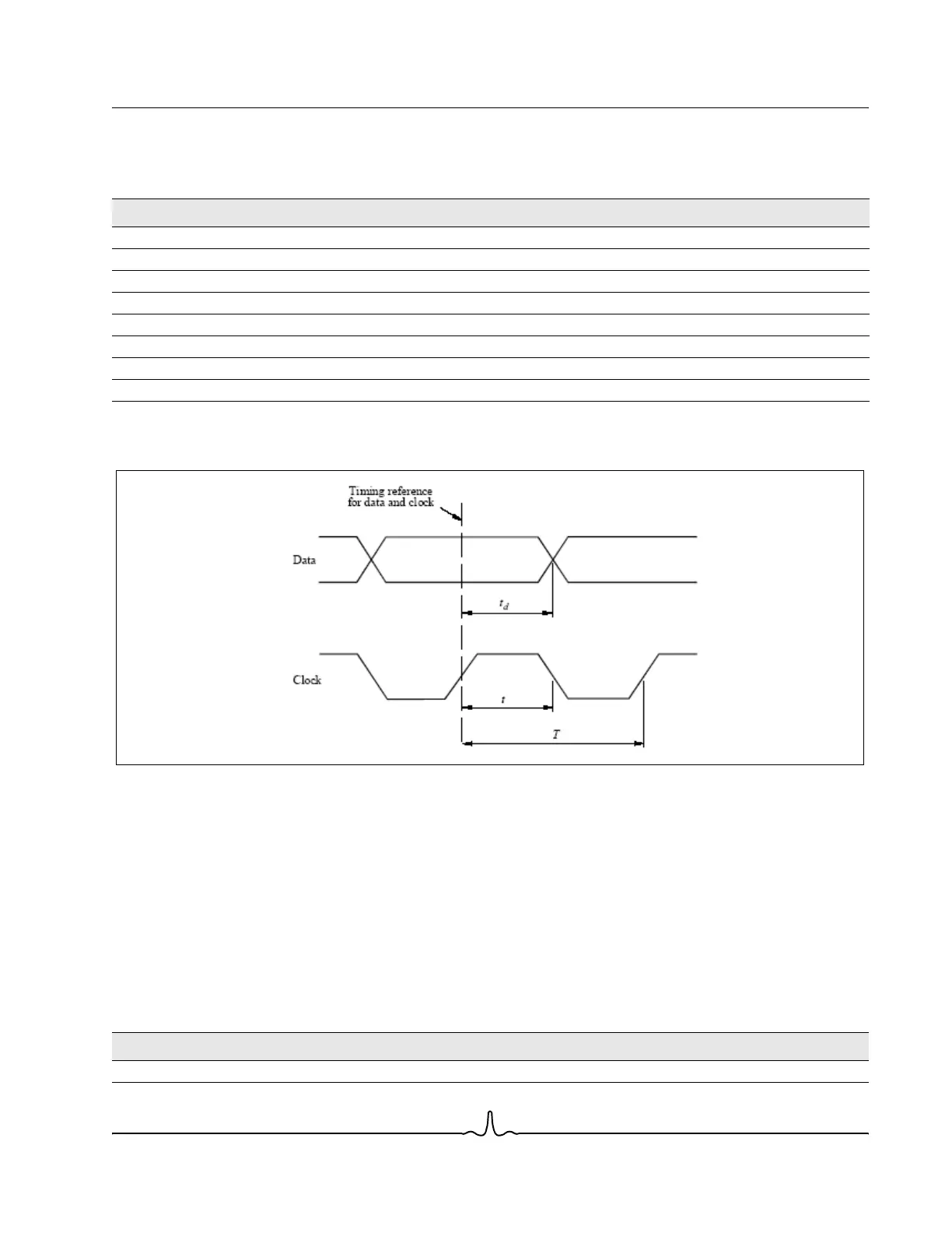
Figure 1-52: Serial Teletext Port Output Timing Diagram
The clock signal is a 27-MHz square wave. The ITU656 output clock is used as the reference clock with the positive transition
of the clock signal occurring midway between data transitions.
• Clock period: T =
37 ns
• Clock pulse width: t = 18.5 ns
• Data timing – sending end: t
d
= 18.5 ± 3 ns
TIMING FOR SERIAL TELETEXT OUTPUT AT RMX_DATA1 PIN
Table 1-37: Timing for Alternate 656 Output at vi0_656 Pins
Pin Timing (td) Min Timing (td) Max
vi0_656_0 17.786 ns 19.494 ns
vi0_656_1 17.862 ns 19.086 ns
vi0_656_2 17.799 ns 19.055 ns
vi0_656_3 17.829 ns 18.920 ns
vi0_656_4 17.966 ns 19.118 ns
vi0_656_5 17.663 ns 18.606 ns
vi0_656_6 17.864 ns 18.862 ns
vi0_656_7 17.885 ns 19.295 ns
Table 1-38: Timing for Serial Teletext Output at rmx_data1 Pin
Pin Timing (td) Min Timing (td) Max
rmx_data1 18.16 ns 18.18 ns