2/24/2008 9T6WP
BCM7405 Preliminary Hardware Data Module
Timing and AC Characteristics 06/29/07
Broadcom Corporation
Page 1-166 ITU656 Output Timing Document 7405-1HDM00-R
ITU656 OUTPUT TIMING
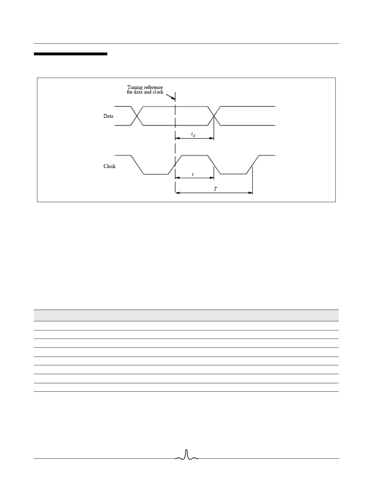
Figure 1-51: ITU656 Output Timing Diagram
The clock signal is a 27-MHz square wave. The positive transition of the clock signal occurs midway between data
transitions.
• Clock period: T = 37 ns
• Clock pulse width: t = 18.5 ns
• Data timing – sending end: t
d
= 18.5 ± 3 ns, based on the ITU-R_BT656-4 specification.
TIMING FOR ITU656 OUTPUT AT VO_656 PINS
Table 1-36: Timing for ITU656 Output at vo_656 Pins
Pin Timing (td) Min Timing (td) Max
vo_656_0 18.118 ns 18.826 ns
vo_656_1 18.162 ns 19.118 ns
vo_656_2 18.186 ns 18.863 ns
vo_656_3 18.111 ns 19.210 ns
vo_656_4 18.160 ns 18.812 ns
vo_656_5 18.148 ns 18.975 ns
vo_656_6 18.078 ns 18.994 ns
vo_656_7 18.200 ns 19.054 ns