2/24/2008 9T6WP
BCM7405 Preliminary Hardware Data Module
Timing and AC Characteristics 06/29/07
Broadcom Corporation
Page 1-152 Data Transport Output Timing Document 7405-1HDM00-R
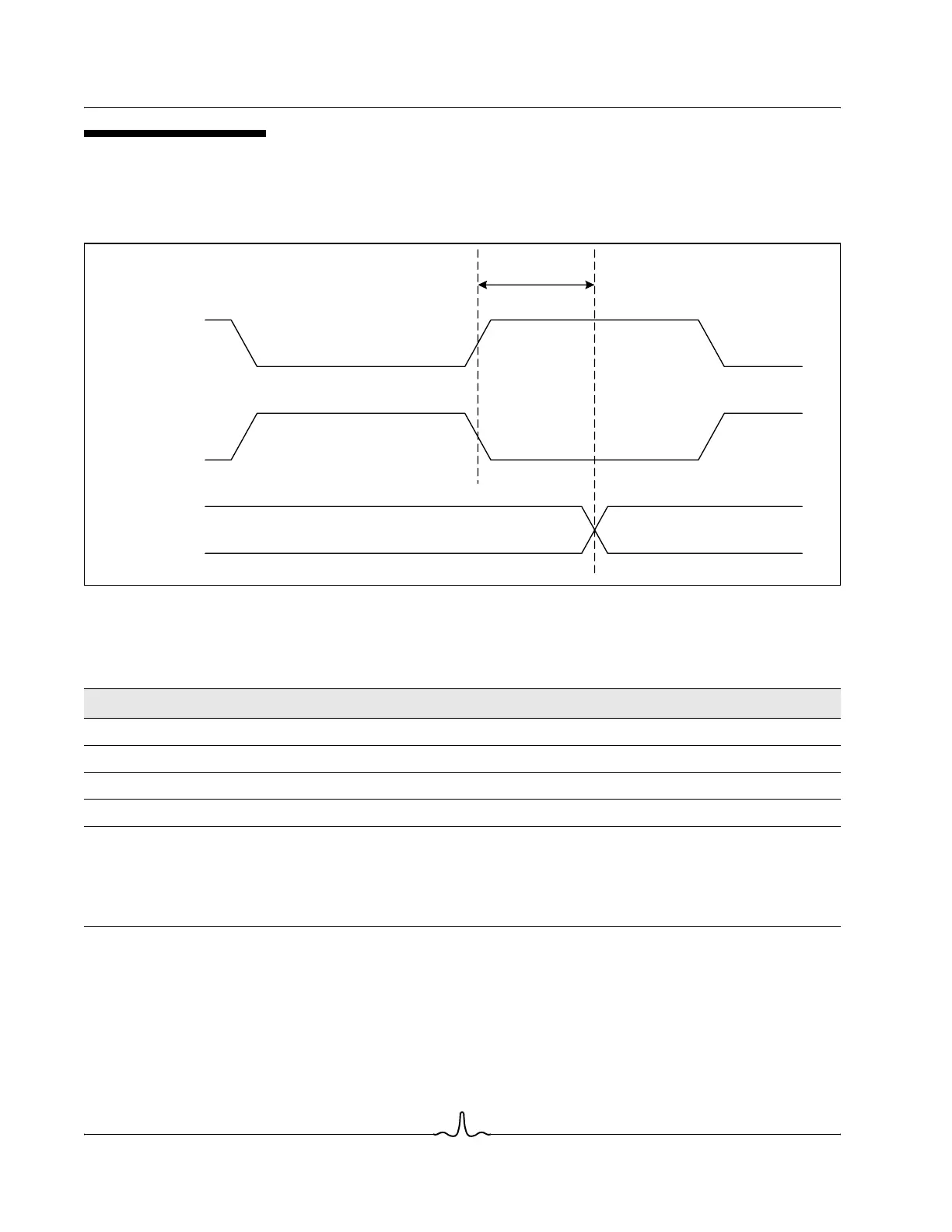
DATA TRANSPORT OUTPUT TIMING
RMX SERIAL OUTPUT PORT TIMING (CLOCK/DATA/SYNC MODE)
Figure 1-37: RMX Serial Output Port Timing (Clock/Data/Sync Mode)
Table 1-23: RMX Serial Output Port Timing (Clock/Data/Sync Mode) Parameters
Description Symbol Min. Max. Units
RMX clock frequency
4
F–81MHz
RMX clock rise time
1,2,4
Trise–2ns
RMX clock fall time
1,2,4
Tfall–2ns
RMX_DATA, RMX_SYNC Output Delay from active clock edge
1,3,4
Tdo(hsx) -3 3 ns
1
All output AC timing is based upon a 20 pF load.
2
Rise and Fall time specs are measured from the 10% and 90% VDD levels.
3
Active clock edge is programmable. Active edge is falling by default, but may be inverted to use rising edge.
4
Tdo are measured from 10% and 90% VDD levels for falling and rising transitions of RMX_DATA and RMX_SYNC
T
do
RMX_CLK
(inverted)
RMX_DATA,
RMX_SYNC
RMX_CLK
(normal)