2/24/2008 9T6WP
BCM7405 Preliminary Hardware Data Module
Timing and AC Characteristics 06/29/07
Broadcom Corporation
Page 1-158 PCI Interface Timing Document 7405-1HDM00-R
PCI INTERFACE TIMING
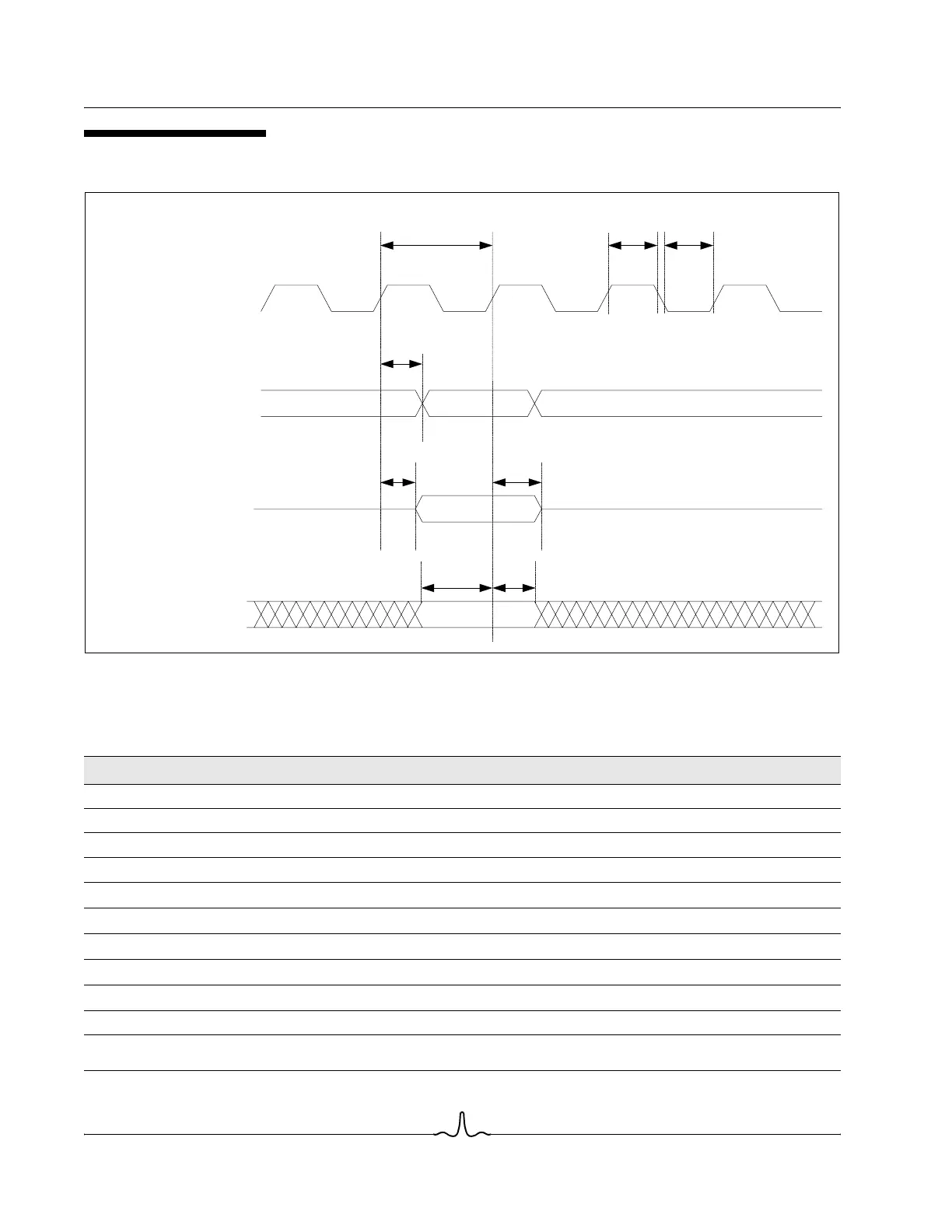
Figure 1-43: PCI Interface Timing Diagram
Table 1-29: PCI Interface Timing Parameters
Description Symbol Min Max Units
PCI CLK Cycle Time T
cyc
30 – ns
PCI CLK High Time T
high
11 – ns
PCI CLK Low Time T
low
11 – ns
PCI CLK to Signal Valid Delay – buses signals
1,2
T
val
211ns
PCI CLK to Signal Valid Delay – point to point signals
1,2
T
val
(ptp) 2 12 ns
Float to Active Delay
1,2
T
on
2– ns
Float to Float Delay
1,2
T
off
–28ns
Input Set up Time to PCI CLK -bused signals
2
T
su
7– ns
Input Set up Time to PCI CLK – point to point signals
2
T
su
(ptp) 10 – ns
Input Hold Time from PCI T
h
0– ns
1. Output delay times are measured with load of 50 pF for 33 MHz on all pins.
2. REQ# and GNT# are point-to-point signals and have different input setup times than do bused signals.
T
cyc
T
high
T
low
T
val
T
on
T
off
T
su
T
h
PCI_CLK
PCI Outputs
PCI Tri-state Outputs
PCI Inputs