A SQUALL II MODULE INTERFACE
5-9
Figure 5-5, Squall II Slave Burst Read Timing Diagram shows 3,1,1,1 clock cycle read; Figure 5-6,
Squall II Slave Burst Write Timing Diagram shows 3,2,2,2 clock cycle write. Any number of wait states
may be run by Squall module slaves.
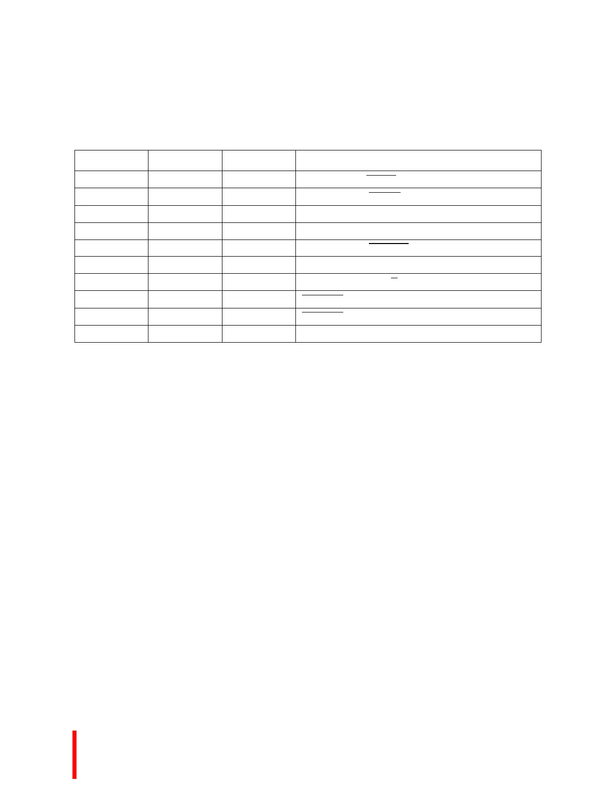
Table 5-4. Squall II Module Slave Timing
Name Minimum Maximum Comment
t1 Note Note Clock to Output S_ADS
t2 2 10 Clock to Output, SQxSEl
t4 10 -- Read S_DATA Setup to Clock
t5 2 -- S_DATA hold from Clock
t6 Note Note Clock to Output, S_BLAST BE[3:0]
t7 Note Note Clock to Output, S_ADDR [31:02]
t8 Note Note Clock to Output, S_W/R
t9 12 -- S_READY Setup to Clock
t10 0 -- S_READY Hold from Clock
t11 Note Note Clock to Output, S_DATA (Write)
NOTE:
Signal timing is dependent on the type of i960 processor and the frequency of operation. Refer to Intel i960 pro-
cessor data sheets for this timing information.