J5 Test/Debug Port Selection
http://www.motorola.com/computer/literature 6-7
6
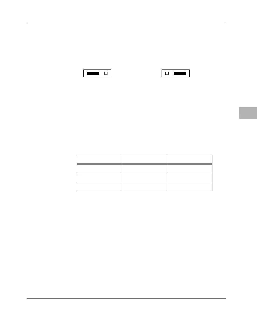
Placing a jumper on J4 pins 1 and 2 designates the 8-bit device in socket
XU1 as the boot source. Placing a jumper on J4 pins 2 and 3 (the default
configuration) designates the 32-bit soldered Flash as the boot source.
J5 Test/Debug Port Selection
Certain MPC821 and MPC860 signal lines have a dual function on the
MBX series embedded controller: they may serve either as IEEE 1149 test
port signals or as Debug port signals, as illustrated in this table.
Placing a jumper on J5 pins 1 and 2 designates the MPC8xx pins listed
above as IEEE 1149 test port signals and enables IEEE 1149 functionality
at the test port header (J23 on the MBX board). Placing a jumper on J5 pins
2 and 3 (the default configuration) designates the MPC8xx pins listed
Boot Port = 32-bit Soldered Flash
(factory configuration)
2148 9802
J4
1 2 3
Boot Port = 8-bit XU1 Device
J4
1 2 3
MPC8xx Pin IEEE 1149 Signal Debug Signal
H16 TCK DSCK
H17 TDI DSDI
G17 TDO DSDO

 Loading...


