Theory of Operation 4-11
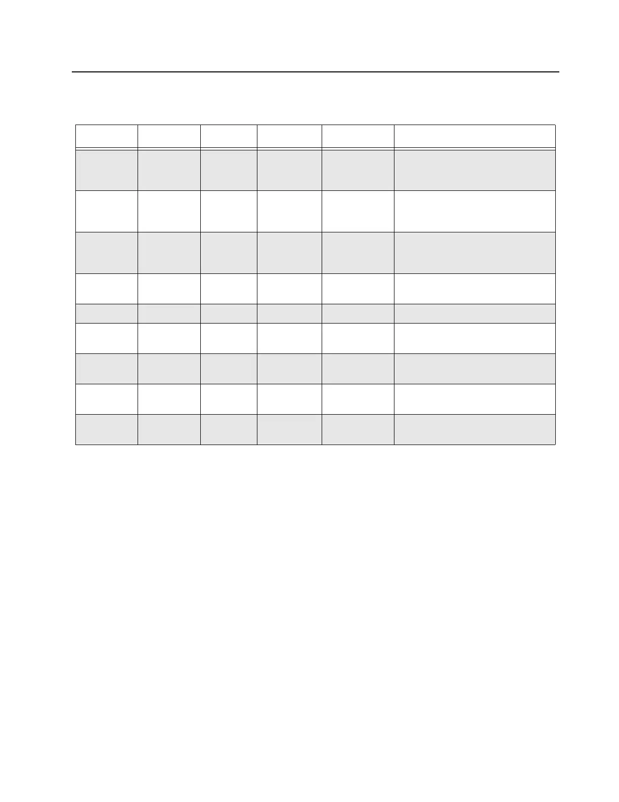
Refer to Table 4-5 for the MAKO general purpose ADC allocation.
4.2.5 Field Programmable Gate Array (FPGA)
The SCM FPGA includes the following major functions:
• External reference watchdog
• SPI Address decoding and buffering
• OCXO and TCXO Phase detection and compensation
• Clock generation
• Reset controller
• External Interface (Wireline SSI, LED, etc.)
FPGA field upgrade capability is also supported on MTR3000 base station/repeater.
Refer to Figure 4-5 for the block diagram of MTR3000 Controller FPGA.
Table 4-5 MAKO General Purpose ADC Allocation
Channel # Metering Module Voltage (V) Value (Hex) Comment
0 Wireline ID MTR3000
Wireline
2.5 0x359 Wireline identification number. Read
during initialization when wireline
module is present.
1 Option1 ID AUX IO 0.373 0x080 AUXIO identification number. Read
during initialization when AUXIO
module is present on Option 1 slot.
2 Option2 ID AUX IO 0.373 0x0BC AUXIO identification number. Read
during initialization when AUXIO
module is present on Option 2 slot.
3 PTEMP+ NA 0.55–2.269 0x0BD–0x30A Peripheral Temp from 3 pin
connector on backplane.
4 RESERVED NA NA NA Pin is reserved for future expansion.
5 14_2V Control 1.79 0x25C For factory to check PS 14.2 V
voltage level.
6 5V Control 1.55 0x20B For factory to check PS 5 V voltage
level.
7 1.875V Control 1.875 0x283 For factory to check main 1.875 V
voltage level.
8 3.3V Control 3.3 0x324 For factory to check main 3.3 V
voltage level.
 Loading...