xiv List of Figures
List of Figures
Figure 1-1 Front view (with front bezel) of MTR3000 Base Station/Repeater ...........1-3
Figure 1-2 Front view (without front bezel) of MTR3000 Base Station/Repeater ......1-3
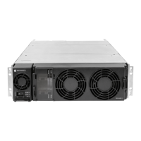
Figure 1-3 Rear view of MTR3000 Base Station/Repeater .......................................1-3
Figure 3-1 PA sub-modules.......................................................................................3-1
Figure 3-2 PA Functional Block Diagram ..................................................................3-3
Figure 3-3 PA DC Power Structure ...........................................................................3-4
Figure 3-4 PA Signal Connectors ..............................................................................3-9
Figure 3-5 Areas to apply thermal grease on the PA metal casting ........................3-10
Figure 3-6 Sequence to tighten back screws on the output board ..........................3-11
Figure 3-7 Sequence to tighten back screws on the distribution board...................3-12
Figure 3-8 Sequence to tighten back screws on the RF board ...............................3-13
Figure 3-9 Fan Troubleshooting Flow Chart (PA)....................................................3-15
Figure 3-10 Power Troubleshooting Flow Chart (PA)................................................3-16
Figure 4-1 MTR3000 Controller Block Diagram ........................................................4-2
Figure 4-2 MTR3000 Controller SPI connection........................................................4-5
Figure 4-3 MTR3000 Controller Clock Configuration ................................................4-9
Figure 4-4 MAKO Block Diagram and usage of MTR3000 Controller .....................4-10
Figure 4-5 MTR3000 Controller FPGA Block Diagram............................................4-12
Figure 4-6 Station Control Module (SCM) Audio Path.............................................4-13
Figure 4-7 MTR3000 Controller Ethernet Connection .............................................4-15
Figure 4-8 USB connector pin-out ...........................................................................4-20
Figure 4-9 MTR3000 power up block diagram ........................................................4-23
Figure 4-10 Controller Troubleshooting Flow Chart ..................................................4-25
Figure 4-11 Power Troubleshooting Flow Chart (Controller).....................................4-26
Figure 4-12 Clock and Reset Troubleshooting Flow Chart (Controller).....................4-27
Figure 4-13 Ethernet Troubleshooting Flow Chart (Controller) .................................4-28
Figure 4-14 Transmit Path Troubleshooting Flow Chart (Controller).........................4-29
Figure 4-15 Receive Path Troubleshooting Flow Chart (Controller)..........................4-30
Figure 4-16 Audio Troubleshooting Flow Chart (Sheet 1 of 2) ..................................4-31
Figure 4-17 Audio Troubleshooting Flow Chart (Sheet 2 of 2) ..................................4-32
Figure 5-1 Measuring 14.2 VDC and 5.1 VDC (other voltmeter probe to chassis)....5-1
Figure 5-2 Pin-out of connector (measuring 14.2 VDC and 5.1 VDC).......................5-2
Figure 5-3 Measuring 14.2 VDC and 28.6 VDC (other voltmeter probe to chassis)..5-2
Figure 5-4 Pin-out of connector (measuring 14.2 VDC and 28.6 VDC).....................5-2
 Loading...