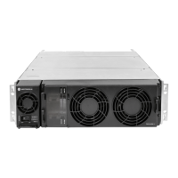
Theory of Operation 4-17
4.2.10 Receiver
The connector (J3601M3) used to connect the controller to the Receiver is a dual row, right angle,
early entry receptacle, without flange, 30-Pin Connector. It provides 16.8 MHz reference clock,
14.2 V, 10 V and 8 V supply voltage, SPI, Abacus SPI/SSI and other digital handshake signals with
the Receiver.
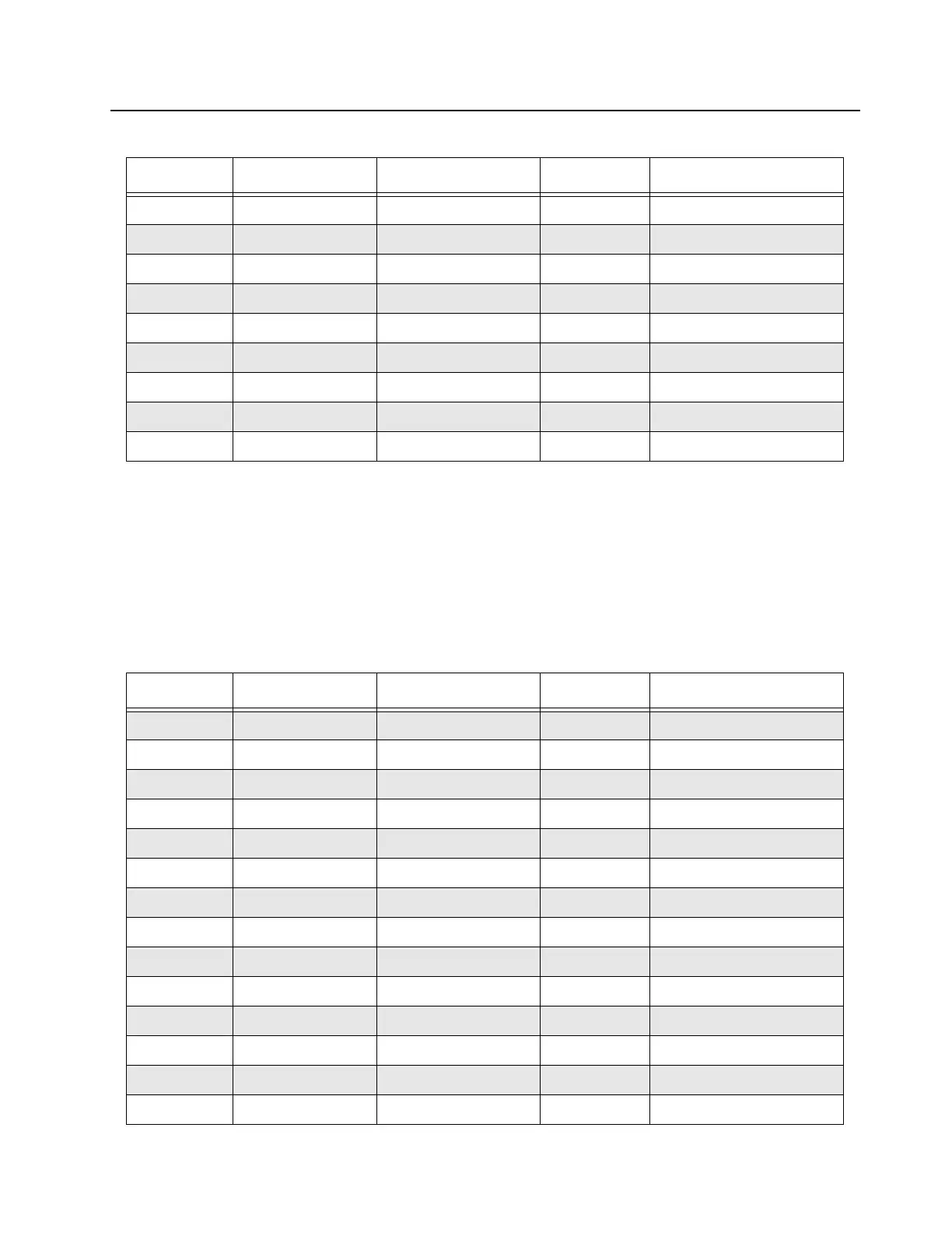
Refer to Table 4-9 for pinout for the Receiver connector.
B7 NC No Connect on Controller
B8 +10V Ex 10.0 V supply 10 V 10VDC
B9 +14_2V Ex 14.2 V supply 14.2 V 14.2VDC
B10 Ground Ground
B11 EX_CPLD_ADD_2 CPLD SPI address 2 3.3 V FPGA
B12 EX_CPLD_ADD_1 CPLD SPI address 1 3.3 V FPGA
B13 EX_CPLD_MOSI CPLD SPI MOSI 3.3 V FPGA
B14 EX_CPLD_MISO CPLD SPI MISO 3.3 V FPGA
B15 NC No Connect on Controller
Table 4-9 MTR3000 Controller Receiver Connector connection
Pin Signal Name Description Signal Level Controller Connection
A1 ABA_ODC Abacus SSI clock 3.3 V Rx OMAP McBSP2.CLKR
A2 Ground Ground
A3 ABA_SYNCB Abacus SYNCB 3.3 V Rx OMAP GPIO40
A4 ABA_PE Abacus SPI chip select 3.3 V FPGA
A5 ABA_PC Abacus SPI clock 3.3 V FPGA
A6 Ground Ground
A7 RX_CPLD_CE CPLD SPI chip select 3.3 V FPGA
A8 RX_CPLD_MISO CPLD SPI MISO 3.3 V FPGA
A9 RX_CPLD_ADD_1 CPLD SPI Address 1 3.3 V FPGA
A10 RX_CPLD_ADD_0 CPLD SPI Address 0 3.3 V FPGA
A11 NC No Connect on Controller
A12 Ground Ground
A13 +10V Rx 10.0 V supply 10 V 10VDC
A14 RX_ATTEN Rx Attenuation Control 3.3 V Rx OMAP GPIO18
Table 4-8 MTR3000 Controller Exciter Connector connection (Continued)
Pin Signal Name Description Signal Level Controller Connection
 Loading...