NE-4100 Series User’s Manual Getting Started
3-8
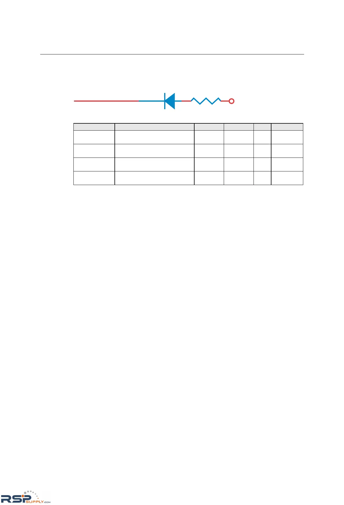
Digital Output LED Circuit Design
The figure shown below is the digital output LED circuit design. This is known as the “sink”
design.
3.3V
Dout
When developing your own applications, you need to be aware of the voltage limits shown below.
Min. Max. Unit Conditions
Low-level
Input Voltage
Maximum voltage when DI is
set to “Low” status.
--- 0.3xVCC V
High-level
Input Voltage
Minimum voltage when DI is
set to “High” status.
0.7xVCC --- V
Low-level
Input Voltage
Maximum voltage when DO is
set to “Low” status.
--- 0.4 V
High-level
Input Voltage
Minimum voltage when DO is
set to “High” status
2.4 --- V
The output current for digital output channels carries only 1 mA.

 Loading...