Table 10. I/O current consumption at VDD_HV_IO = 3.6 V (continued)
Cell VDD_HV_IO
(V)
Load (pF) Period1 (ns) MSCR[OERC] Idde AVG (mA) Idde RMS (mA)
200 130 3 9
50 150 00 1.6 4
200 200 4 11
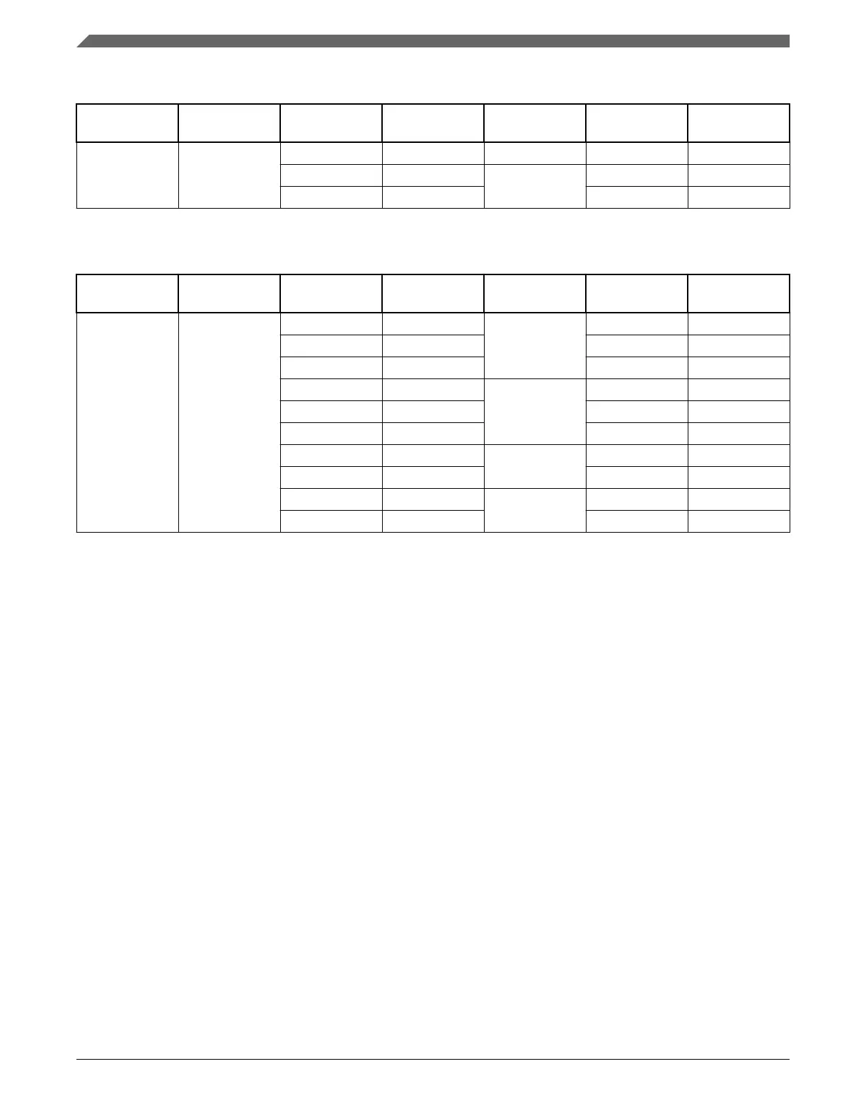
Table 11. I/O current consumption at VDD_HV_IO = 5.5 V
Cell VDD_HV_IO
(V)
Load (pF) Period1 (ns) MSCR[OERC] Idde AVG (mA) Idde RMS (mA)
pad_sr_hv 5.5 25 9 11 37 83
50 10.2 42 89
200 26 46 92
25 10.5 10 25 53
50 16 21 44
200 44 26 49
50 54 01 6 14
200 80 15 35
50 80 00 4 9
200 130 9 22
In order to ensure device reliability, the average current of the I/O on a single segment
should remain below the I
MAXSEG
value given in the table "Absolute maximum ratings".
In order to ensure device functionality, the sum of the dynamic and static current of the
I/O on a single segment should remain below the I
MAXSEG
value given in the table
"Device operating conditions".
Note
The MPC5746R I/O Signal Description and Input Multiplexing
Tables are contained in a Microsoft Excel workbook file
attached to the Reference Manual.
9
Reset pad (PORST, RESET) electrical characteristics
The device implements a dedicated bidirectional reset pin (PORST).
Reset pad (PORST, RESET) electrical characteristics
SPC5746R Microcontroller Data Sheet, Rev. 6, 06/2017
18 NXP Semiconductors

 Loading...


