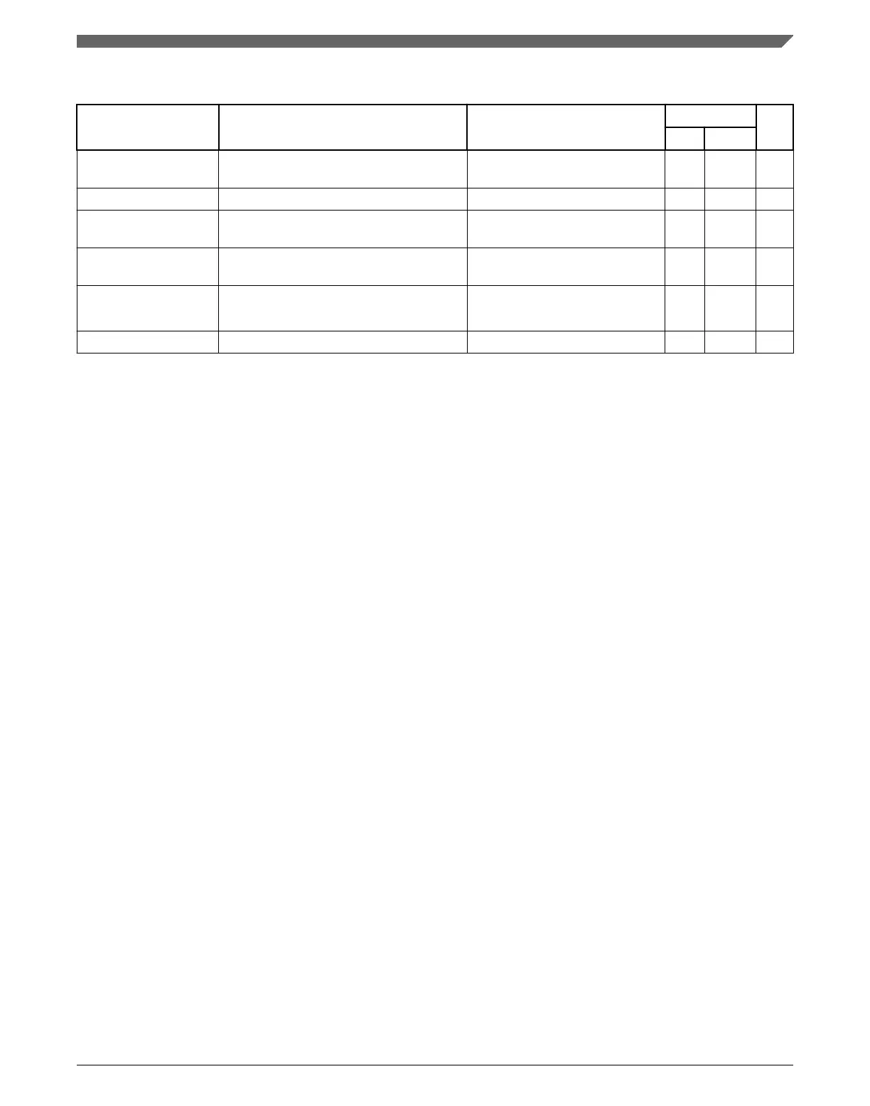
Table 1. Absolute maximum ratings (continued)
Symbol Parameter Conditions
1
Value
Unit
Min Max
I
INJA
Maximum DC injection current for analog
pad
Per pin, applies to all analog pins –5 5 mA
I
MAXSEG
10, 11
Maximum current per I/O segment — –120 120 mA
T
STG
Storage temperature range and non-
operating times
—
–55 175 °C
STORAGE Maximum storage time, assembled part
programmed in ECU
No supply; storage temperature
in range –40 °C to 60 °C
— 20 yrs
T
SDR
Maximum solder temperature
12
Pb-free package
—
— 260 °C
MSL Moisture sensitivity level
13
— — 3 —
1. Voltage is referenced to V
SS
unless otherwise noted.
2. Allowed 1.45 – 1.5 V for 60 seconds cumulative time at maximum T
J
= 150 °C, remaining time as defined in note -1 and
note -1.
3. Allowed 1.375 – 1.45 V for 10 hours cumulative time at maximum T
J
= 150 °C, remaining time as defined in note -1.
4. 1.32 – 1.375 V range allowed periodically for supply with sinusoidal shape and average supply value below 1.275 V at
maximum T
J
= 150 °C.
5. Allowed 5.5 – 6.0 V for 10 hours cumulative time at maximum T
J
= 150 °C, remaining time at or below 5.0 V +10%.
6. Allowed 3.6 – 4.5 V for 10 hours cumulative time at maximum T
J
= 150 °C, remaining time at or below 3.3 V +10%. This is
an internally regulated supply. Values given are for reference only.
7. The maximum input voltage on an I/O pin tracks with the associated I/P supply maximum. For the injection current
condition on a pin, the voltage will be equal to the supply plus the voltage drop across the internal ESD diode from I/O pin
to supply. The diode voltage varies greatly across process and temperature, but a value of 0.3V can be used for nominal
calculations.
8. Relative value can be exceeded, if design measures are taken to ensure injection current limitation (parameters I
INJD
and
I
INJA
).
9. V
DD_HV_IO
/V
SS_HV_IO
refers to supply pins and corresponding grounds: V
DD_HV_IO_MAIN
, V
DD_HV_IO_JTAG
, V
DD_HV_IO_FEC
,
V
DD_HV_IO_MSC
.
10. Sum of all controller pins (including both digital and analog) must not exceed 200 mA. A V
DD_HV_IO
power segment is
defined as one or more GPIO pins located between two V
DD_HV_IO
supply pins.
11. The average current values given in the "I/O pad current specifications" section should be used to calculate total I/O
segment current.
12. Solder profile per IPC/JEDEC J-STD-020D.
13. Moisture sensitivity per JEDEC test method A112.
4 Electromagnetic Compatibility (EMC)
EMC measurements to IC-level IEC standards are available from NXP on request.
5
Electrostatic discharge (ESD)
The following table describes the ESD ratings of the device.
Electromagnetic Compatibility (EMC)
SPC5746R Microcontroller Data Sheet, Rev. 6, 06/2017
NXP Semiconductors 7

 Loading...


