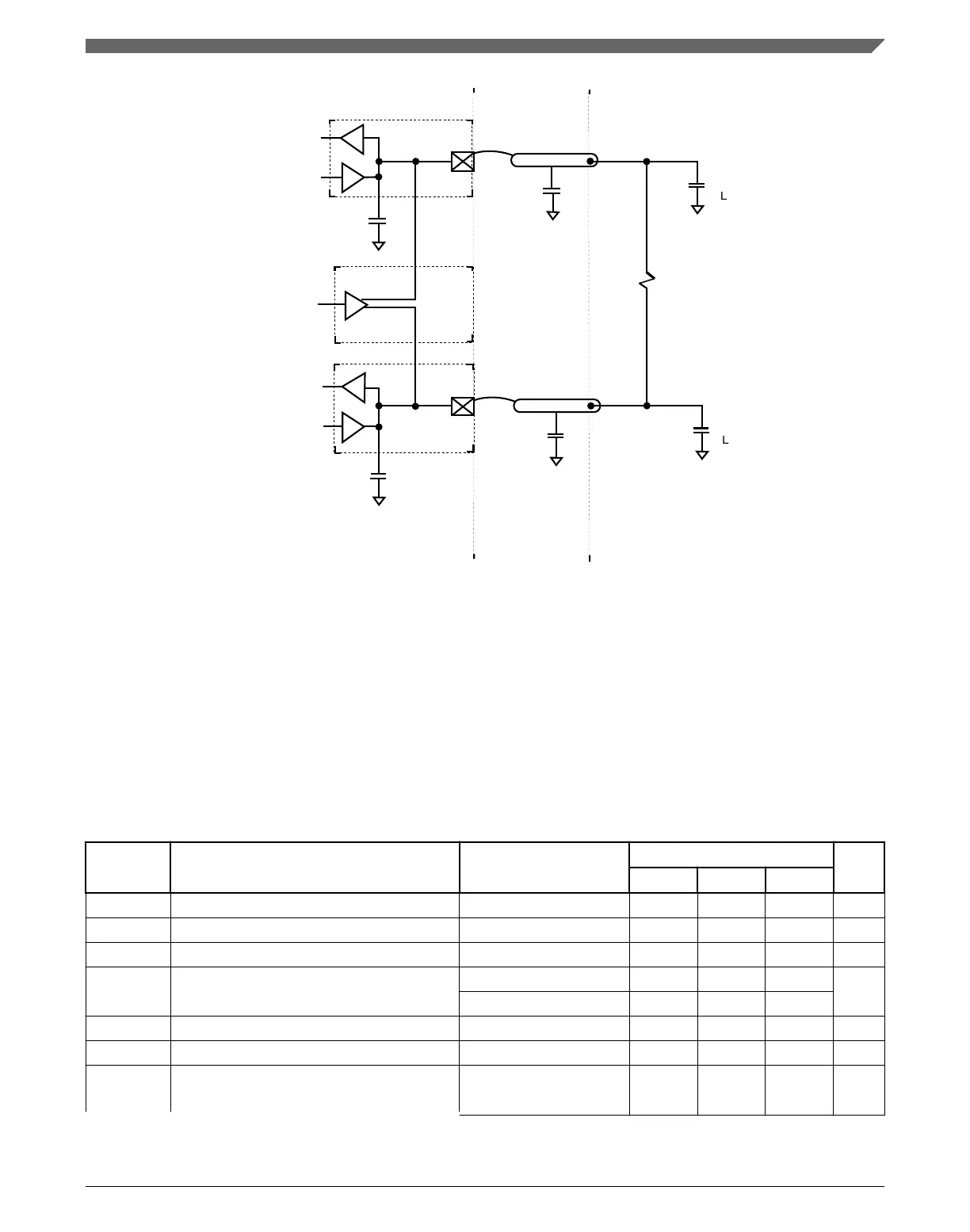
LVDS Driver
GPIO Driver
bond
bond
pad
pad
Die
Package
PCB
C
1pF
1pF
100 Ω
C
termination
2.5pF
2.5pF
L
L
GPIO Driver
Figure 15. LVDS pad external load diagram
14
LFAST PLL electrical characteristics
The following table contains the electrical characteristics for the LFAST PLL.
The specifications in this table apply to both the interprocessor bus and debug LFAST
interfaces.
Table 25. LFAST PLL electrical characteristics
Symbol Parameter Conditions
Value
Unit
Min Nominal Max
f
RF_REF
PLL reference clock frequency — 10 — 26 MHz
ERR
REF
PLL reference clock frequency error — –1 — 1 %
D
CREF
PLL reference clock duty cycle — 45 — 55 %
PN Integrated phase noise (single side band) f
RF_REF
= 20 MHz — — –58 dBc
f
RF_REF
= 10 MHz — — –64
f
VCO
PLL VCO frequency — — 640
1
— MHz
t
LOCK
PLL phase lock
2
— — — 40 µs
ΔPER
REF
Input reference clock single period jitter
(peak to peak)
Single period,
f
RF_REF
= 10 MHz
— — 300 ps
Table continues on the next page...
LFAST PLL electrical characteristics
SPC5746R Microcontroller Data Sheet, Rev. 6, 06/2017
NXP Semiconductors 45

 Loading...


