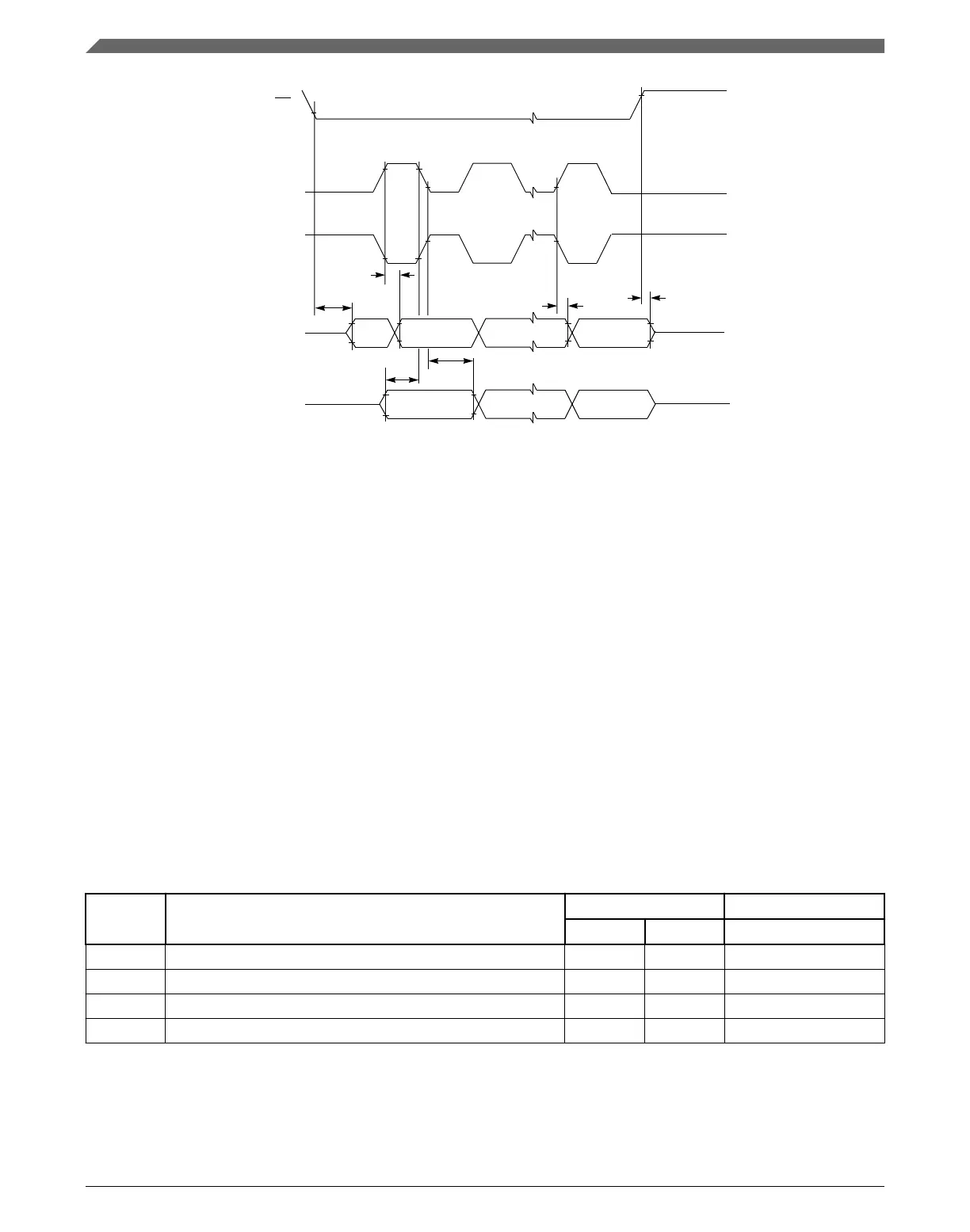
L a s t D a ta
L a s t D a ta
S IN
S O U T
S S
F irs t D a ta
F irs t D a ta
D a ta
D a ta
S C K In p u t
S C K In p u t
(C P O L = 0 )
(C P O L = 1 )
t
A
t
DIS
t
SUI
t
HI
t
SUO
t
HO
Figure 40. DSPI Slave Mode - Modified transfer format timing (MFTE = 0/1) — CPHA = 1
18.3
FEC timing
The FEC supports the 10/100 Mbps MII, 10/100 Mbps MII-lite, and the 10 Mbps-only 7-
wire interface.
18.3.1
MII-lite receive signal timing (RXD[3:0], RX_DV, RX_ER, and
RX_CLK)
The receiver functions correctly up to a RX_CLK maximum frequency of 25 MHz +1%.
There is no minimum frequency requirement. The system clock frequency must be at
least equal to or greater than the RX_CLK frequency.
All timing specifications are referenced from RX_CLK = 1.4 V to the valid input levels.
Table 46. MII-lite receive signal timing
Spec Characteristic
Value Unit
Min Max
M1 RXD[3:0], RX_DV, RX_ER to RX_CLK setup 5 — ns
M2 RX_CLK to RXD[3:0], RX_DV, RX_ER hold 5 — ns
M3 RX_CLK pulse width high 35% 65% RX_CLK period
M4 RX_CLK pulse width low 35% 65% RX_CLK period
AC specifications
SPC5746R Microcontroller Data Sheet, Rev. 6, 06/2017
80 NXP Semiconductors

 Loading...


