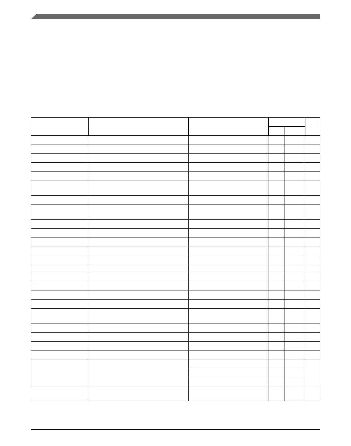
3 Absolute maximum ratings
Functional operating conditions are given in the DC electrical specifications. Absolute
maximum voltages are stress ratings only, and functional operation at the maxima is not
guaranteed. Stress beyond listed maxima may affect device reliability or cause permanent
damage to the device.
Table 1. Absolute maximum ratings
Symbol Parameter Conditions
1
Value
Unit
Min Max
Cycle Lifetime power cycles — 1000k —
V
DD_LV
1.2 V core supply voltage
2, 3, 4
— –0.3 1.5 V
V
DD_LV_BD
Emulation module voltage
2, 3, 4
— –0.3 1.5 V
V
DD_HV_IO_MAIN
I/O supply voltage
5
— –0.3 6.0 V
V
DD_HV_IO_JTAG
Crystal oscillator and JTAG supply Reference to V
SS
–0.3 6.0 V
V
DD_HV_IO_FEC
FEC supply voltage Not using Ethernet Reference to
V
SS
–0.3 6.0 V
V
DD_HV_IO_MSC
MSC supply voltage Reference to V
SS
–0.3 6.0 V
V
DD_HV_PMC
Power Management Controller supply
voltage
6
—
–0.3 6.0 V
V
DD_HV_FLA
Decoupling pin for flash regulator
6
— –0.3 — V
V
DDSTBY
RAM standby supply voltage
6
— –0.3 6.0 V
V
SS_HV_ADV_SD
S/D ADC ground voltage Reference to V
SS
–0.3 0.3 V
V
SS_HV_ADV_SAR
SAR ADC ground voltage Reference to V
SS
–0.3 0.3 V
V
DD_HV_ADV_SAR
SAR ADC supply voltage Reference to V
SS_HV_ADV_SAR
–0.3 6.0 V
V
DD_HV_ADV_SD
S/D ADC supply voltage Reference to V
SS_HV_ADV_SD
–0.3 6.0 V
V
SS_HV_ADR_SD
S/D ADC ground reference Reference to V
SS
–0.3 0.3 V
V
SS_HV_ADR_SAR
SAR ADC ground reference Reference to V
SS
–0.3 0.3 V
V
DD_HV_ADR_SAR
SAR ADC alternate reference Reference to V
SS_HV_ADR_SAR
–0.3 6.0 V
V
DD_HV_ADR_SD
S/D ADC alternate reference Reference to V
SS_HV_ADR_SD
–0.3 6.0 V
V
DD_LV_BD
- V
DD_LV
Emulation module supply differential to 1.2
V core supply
—
–0.3 1.5 V
V
SS
– V
SS_HV_ADR_SAR
V
SS_HV_ADR_SAR
differential voltage — –0.3 0.3 V
V
SS
– V
SS_HV_ADR_SD
V
SS_HV_ADR_SD
differential voltage — –0.3 0.3 V
V
SS
– V
SS_HV_ADV_SAR
V
SS_HV_ADV_SAR
differential voltage — –0.3 0.3 V
V
SS
– V
SS_HV_ADV_SD
V
SS_HV_ADV_SD
differential voltage — –0.3 0.3 V
V
IN
I/O input voltage range
7
— –0.3 6.0 V
Relative to V
SS_HV_IO
, 8, 9
–0.3 —
Relative to V
DD_HV_IO
8, 9
— 0.3
I
INJD
Maximum DC injection current for digital
pad
Per pin, applies to all digital pins –5 5 mA
Table continues on the next page...
Absolute maximum ratings
SPC5746R Microcontroller Data Sheet, Rev. 6, 06/2017
6 NXP Semiconductors

 Loading...


