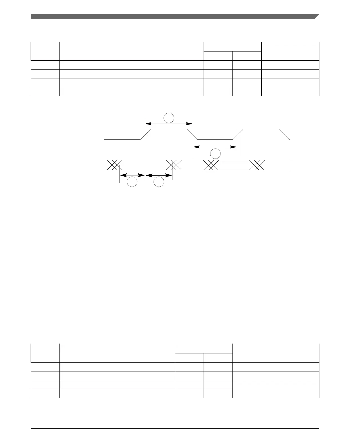
Table 51. RMII receive signal timing
Spec Characteristic
Value Unit
Min Max
R1 RXD[1:0], CRS_DV to REF_CLK setup 4 — ns
R2 REF_CLK to RXD[1:0], CRS_DV hold 2 — ns
R3 REF_CLK pulse width high 35% 65% REF_CLK period
R4 REF_CLK pulse width low 35% 65% REF_CLK period
R2R1
REF_CLK (input)
RXD[1:0] (inputs)
CRS_DV
R3
R4
Figure 46. RMII receive signal timing diagram
18.3.7
RMII transmit signal timing (TXD[1:0], TX_EN)
The transmitter functions correctly up to a REF_CLK maximum frequency of 50 MHz +
1%. There is no minimum frequency requirement. The system clock frequency must be at
least equal to or greater than the TX_CLK frequency, which is half that of the REF_CLK
frequency.
The transmit outputs (TXD[1:0], TX_EN) can be programmed to transition from either
the rising or falling edge of REF_CLK, and the timing is the same in either case. This
options allows the use of non-compliant RMII PHYs.
All timing specifications are referenced from REF_CLK = 1.4 V to the valid output
levels.
Table 52. RMII transmit signal timing
Spec Characteristic
Value Unit
Min Max
R5 REF_CLK to TXD[1:0], TX_EN invalid 2 — ns
R6 REF_CLK to TXD[1:0], TX_EN valid — 16 ns
R7 REF_CLK pulse width high 35% 65% REF_CLK period
R8 REF_CLK pulse width low 35% 65% REF_CLK period
AC specifications
SPC5746R Microcontroller Data Sheet, Rev. 6, 06/2017
NXP Semiconductors 85

 Loading...


