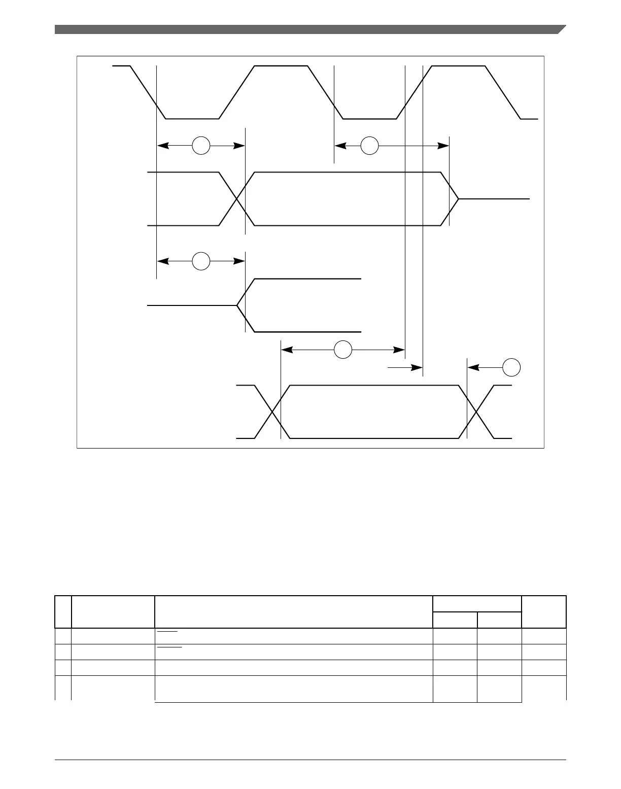
TCK
11
15
14
12
13
Output
Output
Input
Signals
Signals
Signals
Figure 25. JTAG boundary scan timing
18.1.2
Nexus interface timing
Nexus timing specified for the whole V
DD_LV
and V
DD_HV_IO
dynamic, T
A
= T
L
to T
H
,
and maximum loading per pad type as specified in the I/O section of the data sheet.
Table 36. Nexus debug port timing
# Symbol Characteristic
Value Unit
Min Max
1 t
EVTIPW
EVTI Pulse Width 4 — t
CYC
, 1
2 t
EVTOPW
EVTO Pulse Width 40 — ns
3 t
TCYC
TCK cycle time 4
2, 3
— t
CYC
1
4 t
TCYC
Absolute minimum TCK cycle time
4
(TDO sampled on posedge of
TCK)
40
5
— ns
Table continues on the next page...
AC specifications
SPC5746R Microcontroller Data Sheet, Rev. 6, 06/2017
NXP Semiconductors 61

 Loading...


