Table 36. Nexus debug port timing (continued)
# Symbol Characteristic
Value Unit
Min Max
Absolute minimum TCK cycle time
6
(TDO sampled on negedge of
TCK)
20
5
—
5 t
NTDIS
TDI data setup time 5 — ns
6 t
NTDIH
TDI data hold time 5 — ns
7 t
NTMSS
TMS data setup time 5 — ns
8 t
NTMSH
TMS data hold time 5 — ns
9 — TDO propagation delay from falling edge of TCK
7
— 16 ns
10 — TDO hold time with respect to TCK falling edge (minimum TDO
propagation delay)
2.25 — ns
1. t
CYC
is system clock period.
2. Achieving the absolute minimum TCK cycle time may require a maximum clock speed (system frequency / 8) that is less
than the maximum functional capability of the design (system frequency / 4) depending on the actual peripheral frequency
being used. To ensure proper operation TCK frequency should be set to the peripheral frequency divided by a number
greater than or equal to that specified here.
3. This is a functionally allowable feature. However, it may be limited by the maximum frequency specified by the Absolute
minimum TCK period specification.
4. This value is TDO propagation time 36ns + 4ns setup time to sampling edge.
5. This may require a maximum clock speed (system frequency / 8) that is less than the maximum functional capability of the
design (system frequency / 4) depending on the actual system frequency being used.
6. This value is TDO propagation time 16ns + 4ns setup time to sampling edge.
7. Timing includes TCK pad delay, clock tree delay, logic delay and TDO output pad delay.
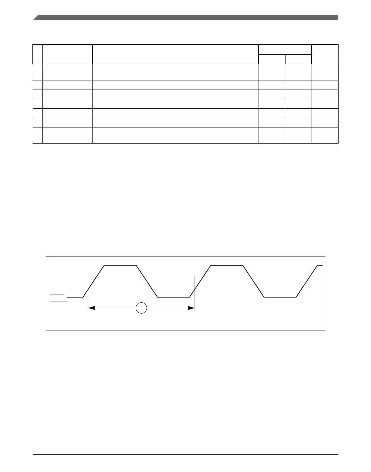
Figure 26. Nexus output timing
Figure 27. Nexus event trigger and test clock timings
AC specifications
SPC5746R Microcontroller Data Sheet, Rev. 6, 06/2017
62 NXP Semiconductors

 Loading...


