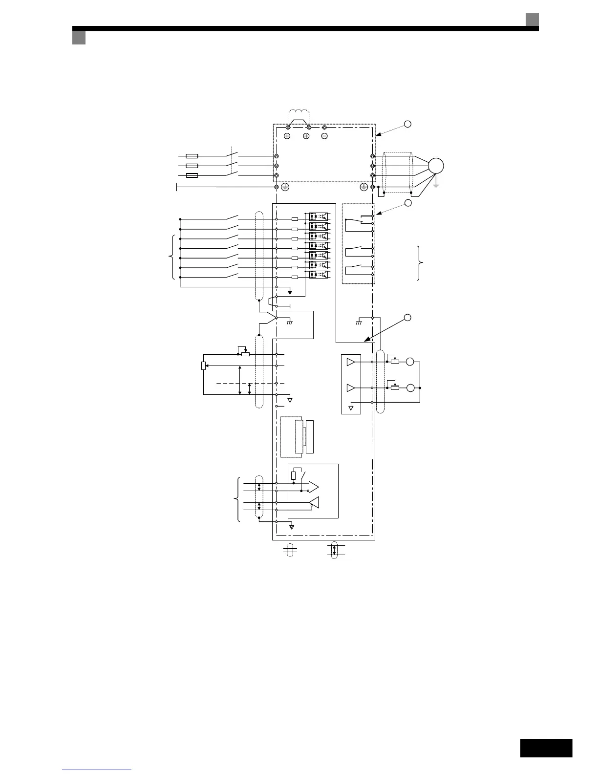
Connection Diagrams
2-3
Fig 2.2 Connection Diagram of IP54 Inverters (Model CIMR-E7Z47P52 Shown Above)
M2
M1
MC
MB
MA
L1
L2
L3
PE
M
R/L1
S/L2
T/L3
U/T1
V/T2
W/T3
E(G)
1 2
UX
Motor
1
2
Main
contactor
3-phase power
supply
380 to 480 V
50/60 Hz
DC reactor to improve input
power factor (optional)
Short-circuit bar
M4
M3
Fault contact output
250 VAC, 1 A max.
30 VDC, 1 A max.
Contact output 1
[Default: During run]
Contact output 2
[Default: Zero speed]
Multi-function digital
output
250 VAC, 1 A max.
30 VDC, 1 A max.
Fuse
Shield
terminal
Varispeed E7
S2
S3
S4
S5
S6
S7
SN
SC
SP
24V
+V
AC
A2
A1
0V
E(G)
PP
4 to 20mA
0 to 10V
3
2k
2
1
-V
Ω
2k
Ω
Reverse Run/Stop
External fault
Fault reset
Multi-step speed setting 1
Multi-step speed setting 2
Jog frequency selection
Multi-function
digital inputs
[Factory settings]
Analog input 1: Master
frequency reference
0 to 10 V (20 k )
Analog input power supply
+15 V, 20 mA
Multi-function analog input 1:
[Default: Frequency Bias
4 to 20 mA (250 )]
Ω
Ω
Analog input power supply
-15 V, 20 mA
Shield
terminal
Adjustment
Forward Run/Stop S1
FM
+
-
AC
FM
Multi-function analog output 1
(0 to 10 V, 2 mA)
[Default: Output frequency, 0 to 10 V]
Multi-function analog output 2
(0 to 10 V, 2 mA)
[Default: Output power, 0 to 10 V]
Ω
Adjustment,
20 k
Ω
+
-
AM
AM
P
Shielded wires
Twisted-pair
shielded wires
Input Option Cards
2CN
R+
R-
S+
S-
IG
P
P
Terminating
resistance
MEMOBUS
communication
RS-485/422
3
Adjustment,
20 k
CIMR-E7Z47P52