ADF SERIES™ OPERATION MANUAL
SECTION 7:
Rear Panel, Connectors and Protection
Entire Contents Copyright 2018 by Pacific Power Source, Inc. (PPS) • All Rights Reserved • No reproduction without written authorization from PPS.
ADF Series Power Source Operation Manual Page 142 of 349
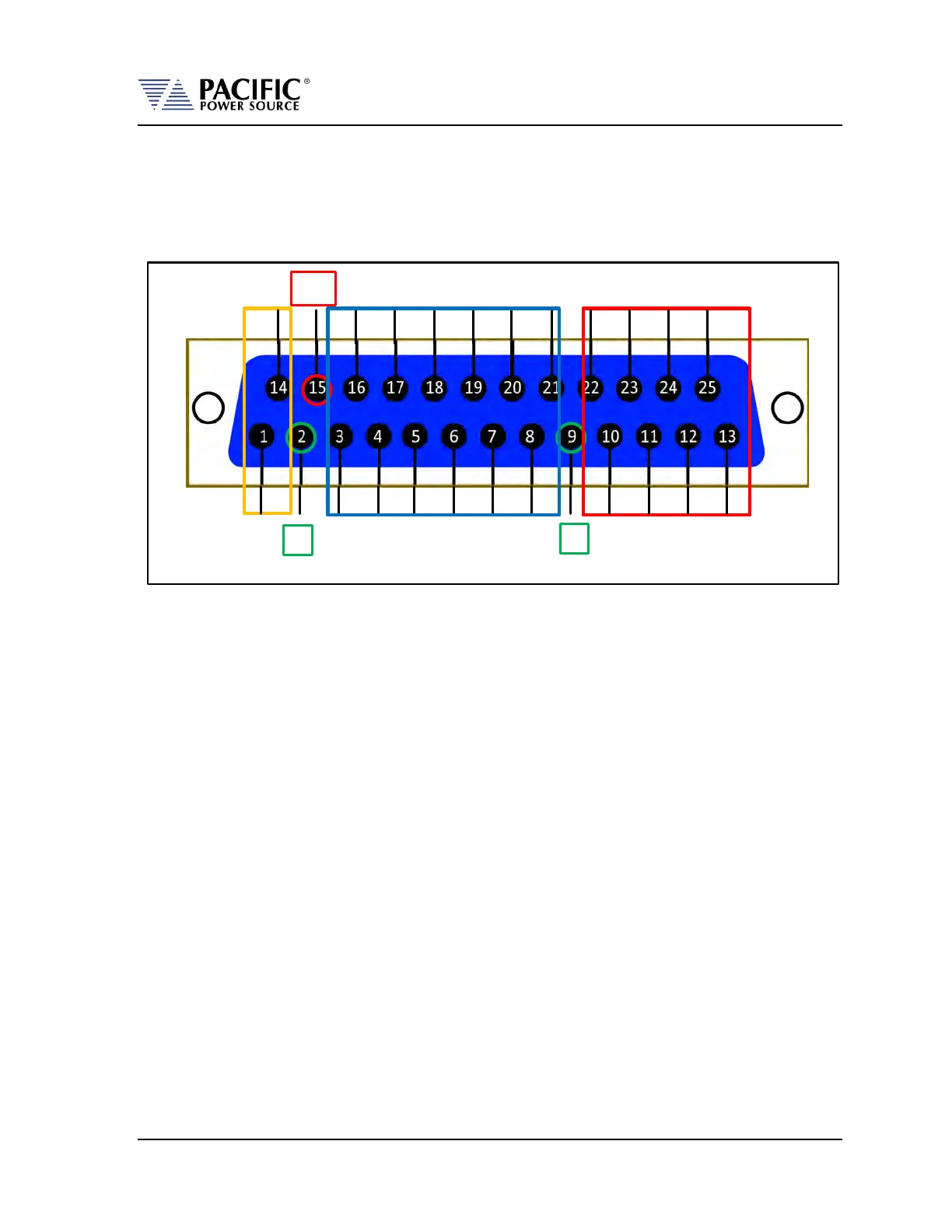
7.3.2 DB25 Connector AUX I/O Pin locations
The pin locations for the various I/O signals on the DB25 connectors are shown in Figure 7-2
below. Note that the connector is installed “Upside” down due to mounting constraints.
PIN# 1 2 3 4 5 6 7 8 9 10 11 12 13
PIN# 14 15 16 17 18 19 20 21 22 23 24 25
RS232
DIGITAL I/O ANALOG I/O
GND
GND
12VDC
Figure 7-2: DB25 Connector AUX I/O Pin Locations
Functional grouping of pins by I/O function is done as shown in the figure above. The left
hand side groups all Analog I/O signals on top on bottom row. The middle section is
reserved for all Digital I/O pins. The RS232 Transmit (Tx) and Receive (Rx) signals are located
on the far right.


 To Next Page