ADF SERIES™ OPERATION MANUAL
SECTION 7:
Rear Panel, Connectors and Protection
Entire Contents Copyright 2018 by Pacific Power Source, Inc. (PPS) • All Rights Reserved • No reproduction without written authorization from PPS.
ADF Series Power Source Operation Manual Page 143 of 349
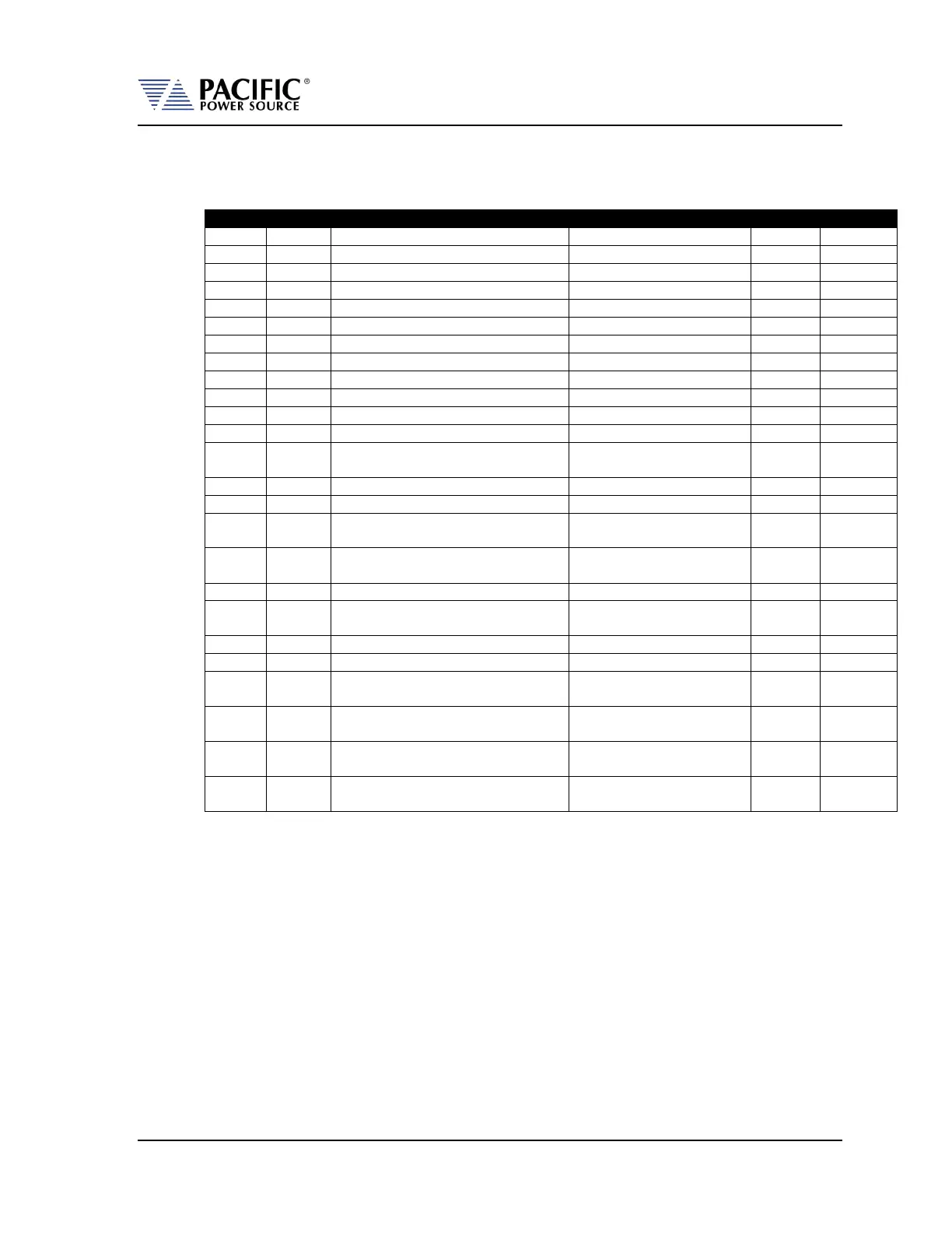
7.3.3 I/O Signal Table by pin number
Pin assignments in order of pin number are shown in the table below.
General Purpose Digital Input #1
General Purpose Digital Input #2
General Purpose Digital Input #3
Analog Input – Volt RMS Phase A
Analog Input – Volt RMS Phase B
Analog Input – Volt RMS Phase C
Analog Input – Current Limit RMS all
phases
0.5 A max, current protected
Programmable, Open
Collector, Current protected
Relay Control #2 - TRANSFORMER
Programmable, Open
Collector, Current protected
Trigger Output / Function Strobe
General Purpose Digital Output #1
General Purpose Digital Output #2
Analog output #1 – Volt RMS
Measurements Phase A
Analog output #2 – Volt RMS
Measurements Phase B
Analog output #3 – Volt RMS
Measurements Phase C
Analog output #4 – Total Power (all
phases combined)
Table 7-1: Auxiliary I/O DB25 Connector Pin numbers and Signals by DB25 pin number