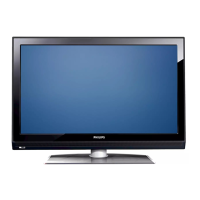
Do you have a question about the Philips 32PFL9432/98 and is the answer not in the manual?
| Screen Size | 32 inches |
|---|---|
| Resolution | 1366 x 768 pixels |
| Display Technology | LCD |
| Backlight Type | CCFL |
| Aspect Ratio | 16:9 |
| Refresh Rate | 50 Hz |
| Brightness | 450 cd/m² |
| Response Time | 8 ms |
| Sound Output | 20 W |
| HDMI Ports | 3 |
| USB Ports | 1 |
| VGA Port | Yes |
| Headphone Jack | Yes |
| Component video (YPbPr/YCbCr) in | 1 |
| SCART ports quantity | 2 |
| S-Video inputs quantity | 1 |
| PC in (D-Sub) | Yes |
| Audio (L/R) in | Yes |
| Audio (L/R) out | Yes |
| Common interface (CI) | Yes |
| RMS rated power | 20 W |
| Number of speakers | 2 |
| Teletext | Yes |
| Viewing Angle, Horizontal | 176 degrees |
| Viewing Angle, Vertical | 176 degrees |
Details about the display's visual characteristics, resolution, color systems, sound, multimedia, and miscellaneous specs.
Explains the various side and rear input/output connectors and their pin configurations for the TV.
Visual guide showing the placement of main circuit boards (PWB/CBA) for different models like 32" and 42" sets.
Outlines essential safety regulations and procedures to follow during repairs, including isolation and component substitution.
Highlights critical warnings regarding electrostatic discharge (ESD), high voltage, and proper component handling.
Provides general notes on measurement conditions, schematic conventions, BGA IC handling, and lead-free soldering.
Illustrates how cables are routed and secured within the chassis for different models (32", 42", 47").
Details how to position the TV for servicing using foam bars or aluminium stands.
Step-by-step instructions for removing the rear cover and various internal panels on ME7 styled sets.
Instructions for removing the rear cover on Aurea styled sets, noting stand removal is not necessary.
Guidelines for reassembling the TV, emphasizing cable routing and EMC foam placement.
Lists key test points and instructions for performing measurements and diagnostics using ICs and test patterns.
Explains how to access Service Default Mode (SDM) and Service Alignment Mode (SAM) for settings and diagnostics.
Explains the start-up sequence and error detection mechanisms for protection states and the transition diagram.
Introduces ComPair as a service tool for diagnostics, troubleshooting, and software upgrades.
Explains the error code buffer, logging mechanisms, error detection types, and methods to read/clear errors.
Explains how to interpret blinking LED codes for error detection when no picture is visible.
Covers software and hardware protections related to power supplies, safety checks, and audio circuits.
Provides fault finding tips for Ambilight, Audio Amplifier, CSM, DC/DC converters, and SSB replacement.
Details the process for upgrading main and stand-by software via USB stick or PC interface.
Illustrates the wiring connections for a 32" LCD TV, showing major component locations and interconnects.
Shows the wiring diagram for 42" LCD models, including DFI and AmbiLight modules with connector details.
Depicts the wiring layout for 47" LCD TVs, incorporating DFI and AmbiLight components and connector assignments.
Illustrates the wiring connections for 42" Aurea styled LCD TVs, detailing DFI and AmbiLight interfaces.
Presents the block diagram for the 32" display supply unit, detailing mains filter, standby, and bias supply circuits.
Details the block diagram for the 37"-42" display supply unit, covering mains filter, standby, and DC-DC conversion stages.
Shows the block diagram for the 47"-52" display supply unit, detailing connector pinouts and power distribution.
Illustrates the block diagram for the audio and Ambilight supply, detailing power distribution and control signals.
Provides a block diagram of the video signal path, including tuner, PNX85xx, PNX5050, and Pacific 3 processing.
Shows the block diagram for the audio signal path, detailing tuner, PNX85xx, and audio output stages.
Illustrates the control signals and clock distribution across various ICs and modules within the system.
Provides a visual overview of test points on the top side of the SSB with grid references for easy identification.
Identifies specific test points on the top side of Part 1 of the SSB.
Identifies specific test points on the top side of Part 2 of the SSB.
Provides a visual overview of test points on the bottom side of the SSB with grid references for easy identification.
Identifies specific test points on the bottom side of Part 1 of the SSB.
Identifies specific test points on the bottom side of Part 2 of the SSB.
Illustrates the I2C communication paths and interconnections between various ICs in the system.
Shows the distribution of power supply lines from various sources to different modules and ICs across the chassis.
Detailed circuit diagram for the first part of the 32" display supply unit, including mains filter and standby.
Detailed circuit diagram for the second part of the 32" display supply unit, covering DC-DC conversion.
Top-side PWB layout for the 32" display supply panel, showing component placement and reference designators.
Bottom-side PWB layout for the 32" display supply panel, indicating component placement and reference designators.
Circuit diagram for the mains filter and standby section of the 42" display supply unit.
Circuit diagram for the main supply section of the 42" display unit, detailing various voltage outputs.
Circuit diagram illustrating the DC-DC conversion stages for the 42" display supply, including boosters.
Top-side PWB layout for the 42" display supply panel, showing component placement and reference designators.
Bottom-side PWB layout for the 42" display supply panel, indicating component placement and reference designators.
Circuit diagram for the DC-DC conversion power stages within the DFI panel.
Illustrates the video signal path and processing blocks within the DFI panel, including LVDS interfaces.
Shows the clock signal distribution and generation circuits within the DFI panel.
Circuit diagram for the power supply section of the DFI panel, detailing voltage regulators.
Circuit diagram detailing the power supply and control interfaces for the DFI FPGA module.
Circuit diagram for the DFI FPGA, illustrating its interfaces to memory and other components.
Circuit diagram showing the DDR A memory interface connections for the DFI panel.
Circuit diagram illustrating the DDR B memory interface connections for the DFI panel.
Circuit diagram detailing the display interface signals, including I2C buffers and control lines.
Circuit diagram for the FPGA responsible for driving the Ambilight units, showing its interfaces.
Circuit diagram for the DFI FPGA, illustrating its interfaces to memory and other components.
Continuation of the DFI FPGA circuit diagram, detailing pin assignments and configuration.
Circuit diagram for the 5-LED AmbiLight panel, showing LED drivers and control circuitry.
Continuation of the circuit diagram for the 5-LED AmbiLight panel, detailing its internal connections.
Top-side PWB layout for the 5-LED AmbiLight panel, showing component placement.
Top-side PWB layout for Part 1 of the 5-LED AmbiLight panel, identifying components.
Top-side PWB layout for Part 2 of the 5-LED AmbiLight panel, showing component placement.
Circuit diagram for the 3-sided, 4-LED AmbiLight panel, detailing driver circuits and interfaces.
Continuation of the circuit diagram for the 3-sided, 4-LED AmbiLight panel, showing driver details.
PWB layout for the top side of the 3x4 LED AmbiLight panel, showing component placement.
Top-side PWB layout for Part 1 of the 3x4 LED AmbiLight panel, identifying components.
Top-side PWB layout for Part 2 of the 3x4 LED AmbiLight panel, showing component placement.
Circuit diagram for the supply section of the Audio & AmbiLight panel (AP1).
Circuit diagram for the left and right audio channels, detailing amplifiers and output stages.
Circuit diagram detailing the audio protection and mute control circuits for the audio system.
Circuit diagram for the audio subwoofer channel, including amplifiers and feedback mechanisms.
Circuit diagram for the centre audio input and subwoofer filter stages, detailing signal paths.
Top-side PWB layout for the Audio & AmbiLight Supply panel (AP1), showing component placement.
Bottom-side PWB layout for the Audio & AmbiLight Supply panel (AP1), indicating component placement.
Circuit diagram for the main SSB supply unit (B01A), detailing its power conversion stages.
Circuit diagram for the auxiliary SSB supply unit (B01B), covering mains filter and standby functions.
Circuit diagram for the DC/DC converter (B02A) responsible for generating various voltages.
Circuit diagram for the DC/DC converter (B02B) responsible for generating various voltages.
Circuit diagram for the DC/DC converter (B02C) responsible for generating various voltages.
Circuit diagram for the channel decoder IC (B03A), detailing its interfaces and internal blocks.
Circuit diagram for the main tuner module (B03B), showing RF input, IF processing, and control signals.
Circuit diagram detailing the control signals and peripherals of the PNX85xx SoC.
Circuit diagram for the PNX85xx debug interface, including JTAG and UART connections.
Circuit diagram showing the NVM and UART switch functions for the PNX85xx processor.
Circuit diagram for miscellaneous functions of the PNX85xx, including power and reset signals.
Circuit diagram detailing the control signals and peripherals of the PNX85xx SoC.
Circuit diagram showing the SDRAM interface connections for the PNX85xx SoC.
Circuit diagram for the digital video input interfaces of the PNX85xx SoC, including HDMI and CMOS.
Circuit diagram for the audio processing subsystem of the PNX85xx SoC, including headphone output.
Circuit diagram for the analogue AV inputs and processing within the PNX85xx SoC.
Circuit diagram for the audio processing subsystem of the PNX85xx SoC, detailing input and output paths.
Further details of the audio subsystem circuit diagram for the PNX85xx SoC, showing driver details.
Circuit diagram illustrating the video stream handling and multiplexing within the PNX85xx SoC.
Circuit diagram for the digital video output and LVDS interfaces of the PNX85xx SoC.
Circuit diagram for the power supply management and voltage regulation for the PNX85xx SoC.
Circuit diagram for the flash memory interface of the PNX85xx SoC, showing connections to NAND flash.
Circuit diagram for the control functions of the PNX5050 video backend processor, including PCI interface.
Circuit diagram showing the SDRAM interface connections for the PNX5050 processor.
Circuit diagram for the video processing functions of the PNX5050 processor, including inputs and outputs.
Circuit diagram for the power supply section of the PNX5050 processor, detailing voltage regulators.
Circuit diagram illustrating the LVDS interfaces for the Pacific 3 chip, covering single and dual modes.
Circuit diagram for the display interface and I2C buffers connected to the Pacific 3 chip.
Circuit diagram detailing the control signals and interface for the Pacific 3 chip, including JTAG.
Circuit diagram for the UART interface, including service connector and debug connections.
Circuit diagram for the SPDIF audio interface, showing signal routing and buffer circuits.
Circuit diagram for analogue external I/O connections, including CVBS, Y/C, and audio inputs.
Circuit diagram illustrating the HDMI switch and EDID NVM interfaces for signal routing.
Circuit diagram showing the debug interface connections and RS232 interface for service access.
Circuit diagram detailing the control signals and peripherals of the PNX85xx SoC.
Circuit diagram for analogue external I/O connections, including CVBS, Y/C, and audio inputs.
Circuit diagram for analogue external connections, including audio inputs and headphone output.
Circuit diagram for the digital video input interfaces of the PNX85xx SoC, including HDMI and CMOS.
Circuit diagram for the USB 2.0 controller and connector, showing power and data lines.
Circuit diagram for the LED panel connector, detailing signal assignments and power connections.
Circuit diagram for the left and right audio channels, including amplifier stages and output connections.
Circuit diagram detailing the audio protection and mute control circuits, including comparators and transistors.
Explanation of the Service Reference Protocol (SRP) symbols and signal naming conventions used in schematics.
Continuation of the SRP list, detailing various signal references and their schematic locations for troubleshooting.
Overview of the Small Signal Board (SSB) top-side layout, showing the placement of major ICs and connectors.
Top-side PWB layout for Part 1 of the Small Signal Board (SSB), indicating component placement.
Top-side PWB layout for Part 2 of the Small Signal Board (SSB), showing component placement.
Overview of the Small Signal Board (SSB) bottom-side layout, showing component placement and reference designators.
Bottom-side PWB layout for Part 1 of the Small Signal Board (SSB), indicating component placement.
Bottom-side PWB layout for Part 2 of the Small Signal Board (SSB), showing component placement.
Circuit diagram for the Side I/O panel, detailing its connectors and functions.
Top-side PWB layout for the Side I/O panel, showing component placement.
Bottom-side PWB layout for the Side I/O panel, indicating component placement.
Circuit diagram for the keyboard control panel, including button functions and diversity resistors.
Top-side PWB layout for the Keyboard Control Panel, showing component placement.
Bottom-side PWB layout for the Keyboard Control Panel, indicating component placement.
Top-side PWB layout for the Keyboard Control Panel in Aurea models, showing component placement.
Bottom-side PWB layout for the Keyboard Control Panel in Aurea models, indicating component placement.
Circuit diagram for the Front IR and LED panel, showing connections and components.
Top-side PWB layout for the Front IR / LED Panel, showing component placement.
Bottom-side PWB layout for the Front IR / LED Panel, indicating component placement.
Circuit diagram and PWB layout for the IR & LED Panel used in Aurea models.
Specifies general electrical conditions, test signals, and tool requirements for performing alignments.
States that hardware alignments are not applicable for this specific chassis model.
Explains how to access and perform software alignments using the SAM menu for various parameters.
Explains the microprocessor's communication with I2C ICs via option codes for system configuration.
Explains how to set options using numerical strings and refers to external stickers for correct values.
Provides a table detailing option codes for different CTN models, linking them to display settings.
Emphasizes the importance of resetting the NVM on repaired SSBs and setting default values for proper operation.
Introduces the chassis, its platform, and the main ICs involved in video and audio processing.
Lists key features including resolution, Perfect Pixel HD, LED AmbiLight, ClearLCD, DFI, and Digital Natural Motion.
Shows the physical layout of the SSB components on both the top and bottom sides for easy identification.
Details the platform power management system, including standby, semi-standby, and active modes.
Describes the display supply units for different set sizes (32", 42", 47"), including their functions and voltages.
Describes the platform power management system, including voltage rails, signals, and their operation.
Explains the operation of DC/DC converters, including PSU start-up sequence and internal protections.
Details the device specifications for the Tuner, Master IF, SAW filter, and Channel Decoder ICs.
Describes the PNX85xx SoC functions, including video subsystem, audio subsystem, and control subsystems.
Refers to block diagrams for PNX85xx, PNX5050, Pacific 3, and Ambilight FPGA components.
Explains the output signal path for HD sets, including PNX5050, Pacific 3, and Ambilight unit control.
Details the signal path for Full-HD sets, including the use of DFI panel for upscaling and backlight dimming.
Explains the role of the DFI panel in achieving 100 Hz refresh rate for full-HD sets and its interfaces.
Describes the PNX85xx outputs to Pacific 3 and CMOS interfaces to PNX5050 or Cyclone II for video processing.
Details the tasks performed by PNX5050, including picture quality improvement and video mixing.
Explains the functions of the PACIFIC 3 chip, such as color processing, backlight dimming, and pattern generation.
Details the DFI FPGA's role in upconverting signals to 100 Hz and its interfaces.
Explains the system for LED Ambilight units, their addressing, and driving mechanisms.
Provides an alphabetical list of abbreviations and their meanings used throughout the manual for clarity.
Shows internal block diagrams and pin configurations for key ICs used in the chassis.





 Loading...