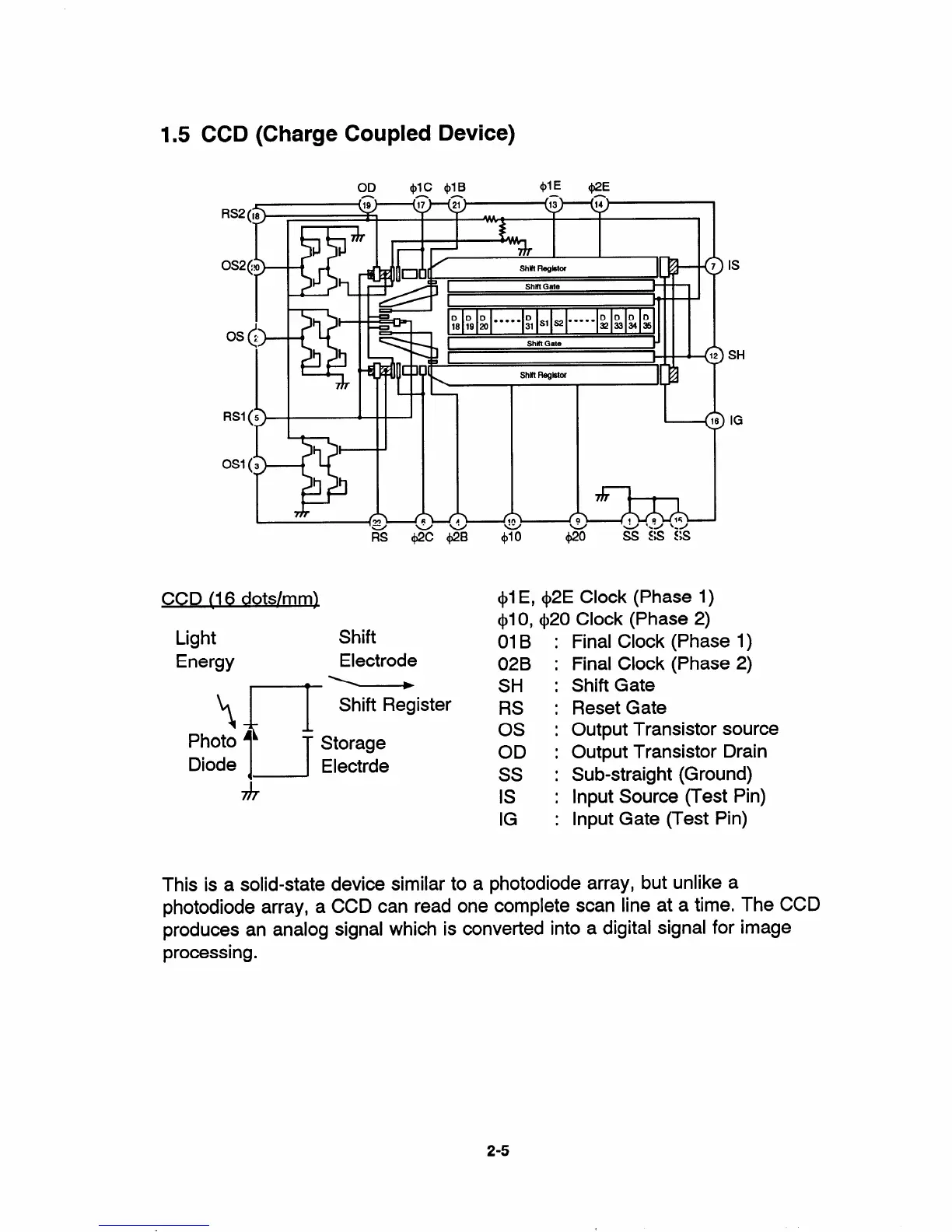
1.5 CCD (Charge Coupled Device)
OD
t$~C IJ)~B
@E WE
F
RS2 (la
os2@
0s <>
I
Is
SH
RSI (
0s1 (
Jt
16 IG
CCD (16 dotslm
ml
Light
Shift
Energy
Electrode
~{ 1
Shift Register
Photo 1
T Storage
Diode ~, ] Electrde
.
.
.
,
,
,
,
.
m
●
*
,
,
.
,
.
.
.
$1 E, $2E Clock (Phase 1)
@lO, @20 Clock (Phase 2)
01 B
02B
SH
RS
0s
OD
Ss
Is
IG
Final Clock (Phase
Final Clock (Phase
Shift Gate
Reset Gate
1)
2)
Output Transistor source
Output Transistor Drain
Sub-straight (Ground)
Input Source (Test Pin)
Input Gate (Test Pin)
This is
a solid-state device similar to a photodiode array, but unlike a
photodiode array, a CCD can read one complete scan line at a time. The CCD
produces an analog signal which is converted into a digital signal for image
processing.
2-5


 To Next Page