© by SEMIKRON / 2017-09-07 / Technical Explanation / SKiiP
4
Page 50/73
7.3 Maximum blocking voltage and snubber capacitors
The maximum blocking voltage V
CES
/V
RRM
which is given in the SKiiP
®
4 datasheet must not be exceeded. It
must also be considered that the IGBT switches faster when the junction temperature is low. Suitable
countermeasures are low inductive DC-link designs to keep the overvoltage at the semiconductors low
among others like the application of snubber capacitors, which should be mounted directly on the DC-link
terminals of each half bridge module. The application note AN-7006 “Peak voltage measurement and
snubber capacitor specification” provides information how to perform tests in practice and to select the
snubber capacitors. The following snubber capacitors have been designed for SKiiP
®
4. But nevertheless it
has to be validated by testing that the capacitors are compatible with the design and that they will not be
overloaded.
Table 7—1: Snubber capacitors for
SKiiP
®
4
Capacitance / DC
voltage
For use with
680 nF / 1000V 1200V device
330 nF / 1600V 1700V device
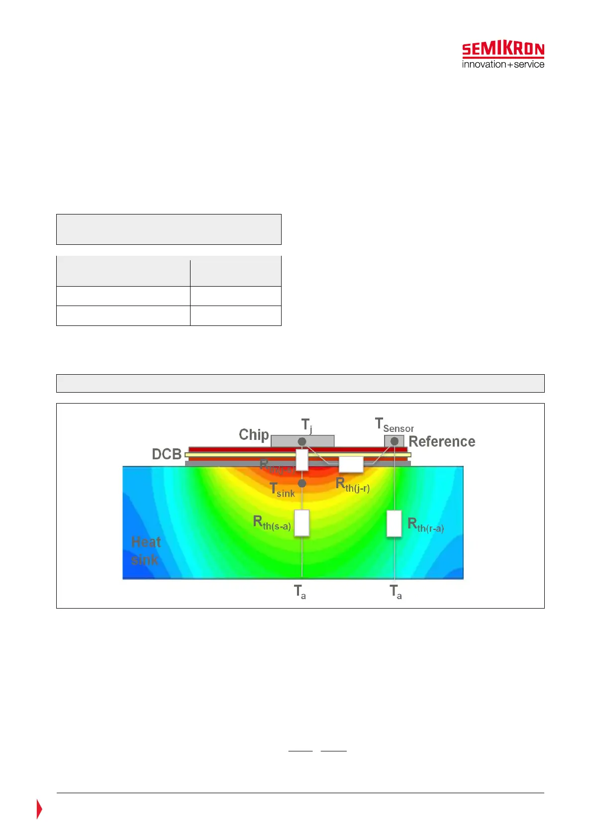
7.4 Definition of Thermal Resistance
The definition of the thermal resistances given in the SKiiP
®
4 datasheet are shown in the Figure 7.2
Figure 7.2: Definition of thermal resistances
T
j
junction temperature of the hottest chip
T
sensor
DCB-sensor temperature
T
sink
heat sink temperature in a drill hole 2mm underneath the chip
T
a
ambient temperature (coolant air or liquid)
R
th
(j-r) thermal resistance between junction and reference
R
th
(j-s) thermal resistance between junction and heat sink
R
th
(s-a) thermal resistance between heat sink and ambient
R
th
(r-a) thermal resistance between reference and ambient
P
losses
Power losses of the chip
In general, the thermal resistance between two points 1 and 2 is defined according to following equation:
losseslosses
th
P
TT
P
T
R
21
)21(
−
=
∆
=
−