© by SEMIKRON / 2017-09-07 / Technical Explanation / SKiiP
4
Page 2/73
Table of Contents
1.
Related documents ..................................................................................................................... 4
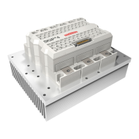
2.
Introduction ............................................................................................................................... 5
2.1
Heat sink ............................................................................................................................. 6
2.2
Power section ....................................................................................................................... 6
2.3
Gate Drive Unit ..................................................................................................................... 7
3.
Topologies and selection guide ..................................................................................................... 8
3.1
Type Designation Code .......................................................................................................... 8
3.2
Overview of the available types and current ratings ................................................................... 9
4.
Standards and qualification tests ................................................................................................ 10
4.1
Tests for qualification and re-qualification............................................................................... 10
4.2
Electromagnetic compatibility (EMC) ...................................................................................... 10
4.3
Isolation coordination .......................................................................................................... 11
4.4
Installation altitude ............................................................................................................. 11
5.
Gate Driver Board..................................................................................................................... 15
5.1
Overview ............................................................................................................................ 15
5.2
Gate driver interface “SKiFace” ............................................................................................. 16
5.2.1
Overview ..................................................................................................................... 16
5.2.2
Pin description .............................................................................................................. 17
5.2.3
External Power Supply ................................................................................................... 20
5.2.4
Switching Signal Inputs ................................................................................................. 21
5.2.5
Analogue Output Signals ................................................................................................ 22
5.2.6
HALT Logic Signal ......................................................................................................... 24
5.2.7
CMN_GPIO1 signal ........................................................................................................ 26
5.2.8
CANbus interface .......................................................................................................... 27
5.2.9
Ground connection ........................................................................................................ 29
5.2.10
Shield and protective earth/chassis connection ................................................................. 29
5.2.11
Reserved or not used signals .......................................................................................... 30
5.3
Gate driver board ................................................................................................................ 31
5.3.1
Overview ..................................................................................................................... 31
5.3.2
Digital signal transmission .............................................................................................. 31
5.3.3
Power-On-Reset ............................................................................................................ 31
5.3.4
Interlock Dead Time Generation ...................................................................................... 32
5.3.5
Short pulse suppression ................................................................................................. 32
5.3.6
IntelliOff ...................................................................................................................... 33
5.3.7
Error Management ........................................................................................................ 35
5.3.8
Analogue signals / sensor functionality ............................................................................ 38
6.
Power terminals ....................................................................................................................... 46
6.1
Electrical limits.................................................................................................................... 46
6.2
Mechanical constraints ......................................................................................................... 46
6.3
Torque at terminal connections ............................................................................................. 46
7.
Application hints ....................................................................................................................... 49
7.1
Verification of design ........................................................................................................... 49
7.2
Safe Operating Area for SKiiP
®
4 ............................................................................................ 49
7.3
Maximum blocking voltage and snubber capacitors .................................................................. 50
7.4
Definition of Thermal Resistance ........................................................................................... 50
7.5
Cooling and coolant circuit .................................................................................................... 51
7.5.1
Materials used and fluid composition ............................................................................... 51
7.5.2
Water connection description of water-cooled SKiiP
®
4 ....................................................... 53
7.6
Isolation voltage test (IVT) ................................................................................................... 55
7.7
FRT (Fault Ride Through) - Function ...................................................................................... 56
7.8
Solar function ..................................................................................................................... 59
7.9
Recommended temperature rating ........................................................................................ 60
7.10
Switching operation and current sharing between paralleled half bridge modules ........................ 63
7.11
Paralleling of SKiiP
®
4 ........................................................................................................... 63