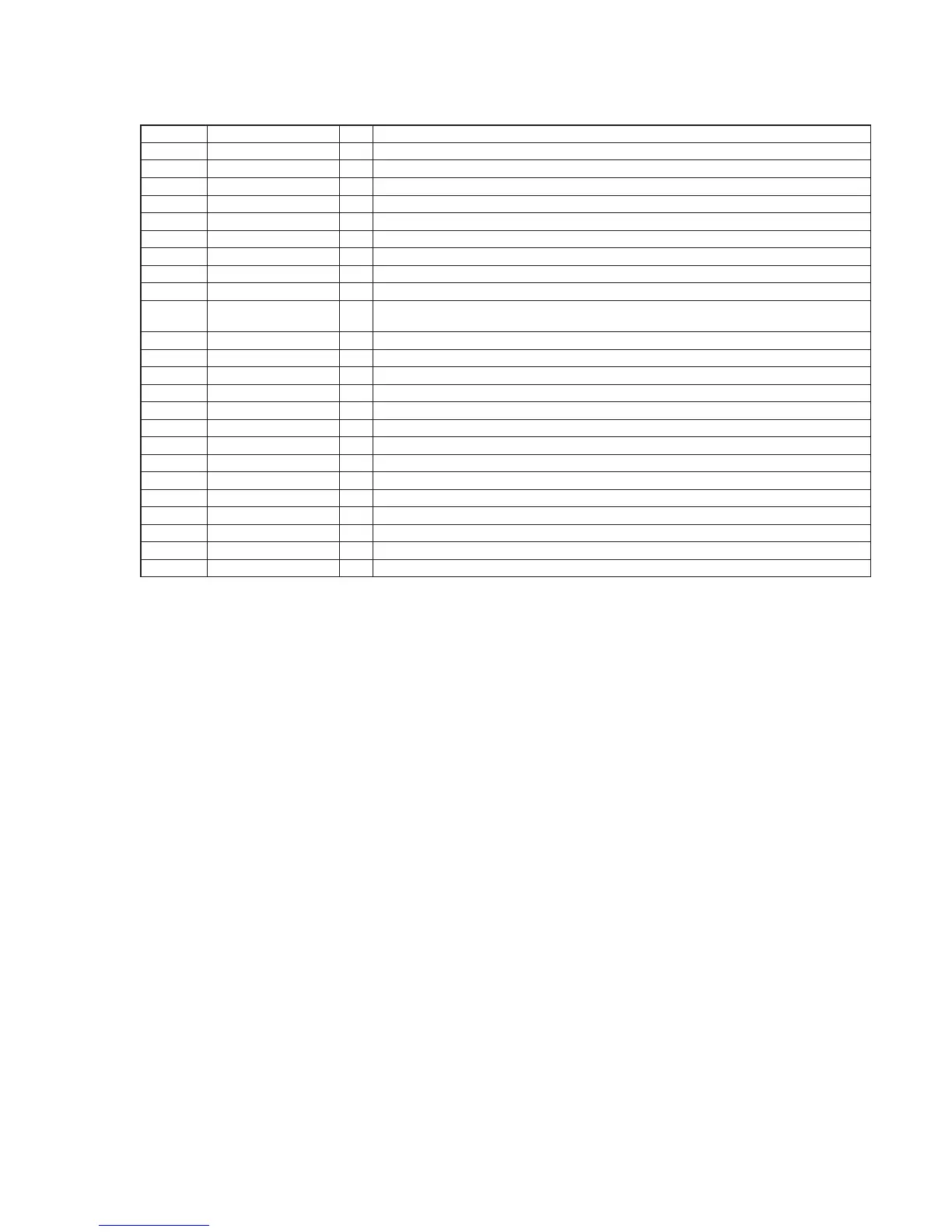
HAP-S1
101
Pin No. Pin Name I/O Description
1 CLOCK I 6 MHz clock signal input terminal
2 VPLL - Power supply terminal for the PLL (+1.2V)
3 GND_3 - Ground terminal
4 VD_4 - Power supply terminal for the digital core and memory (+1.2V)
5 VL_5 - Power supply terminal for the digital interface (+3.3V)
6 CLK/SCL I Serial data transfer clock signal input from the FPGA
7 nCS I Chip select signal input from the FPGA
8 MISO/SDA O Serial data output to the FPGA
9 MOSI I Serial data input from the FPGA
10
nBUSY/HS0/
nEE_CS
O Busy signal output to the FPGA
11 nINT/HS1 O Interrupt signal output to the FPGA
12 nRESET I Reset signal input from the FPGA “L”: reset
13 DBCK - Not used
14 VL_14 - Power supply terminal for the digital interface (+3.3V)
15 GND_15 - Ground terminal
16 VD_16 - Power supply terminal for the digital core and memory (+1.2V)
17 DBDA - Not used
18 MCLK I Master clock signal input terminal Not used
19 DAO_D1 O Audio data output to the FPGA
20 DAO_LRCLK I L/R sampling clock signal input from the FPGA
21 DAO_SCLK I Bit clock signal input from the FPGA
22 DAI_D1 I Audio data input from the FPGA
23 DAI_LRCLK I L/R sampling clock signal input from the FPGA
24 DAI_SCLK I Bit clock signal input from the FPGA
FPGA DSP BOARD IC702 CS48L10-CNZR (AUDIO DSP)
 Loading...