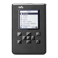
HAP-S1
91
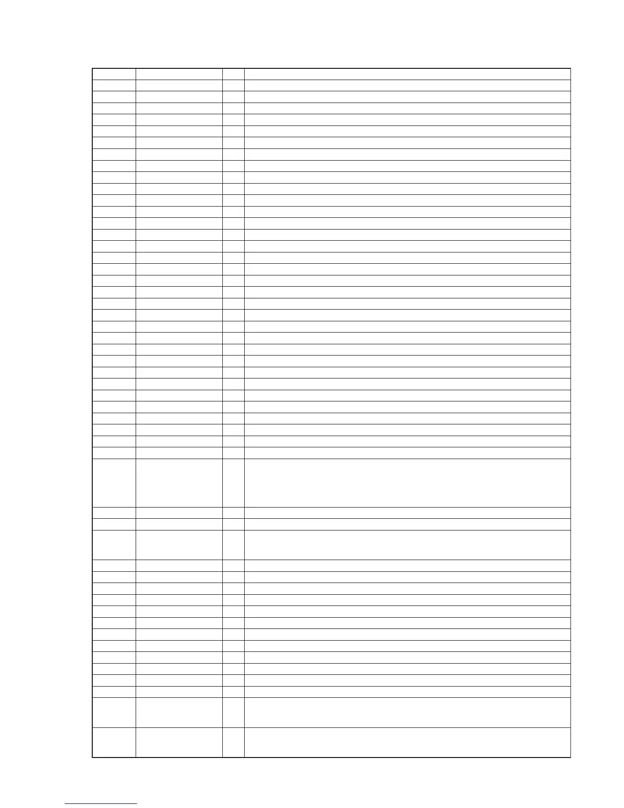
Pin No. Pin Name I/O Description
N11 VDDARM23_CAP6 O Internal regulator output terminal Not used
N12 VDD_CACHE_CAP O Internal regulator output terminal (+1.1V)
N13 VDDARM_CAP6 O Internal regulator output terminal
N14 VDDARM_IN6 - Power supply terminal for the cores regulator (+1.42V)
N15 GND67 - Ground terminal
N16 VDDSOC_IN6 - Power supply terminal for the SOC and PU regulators (+1.42V)
N17 VDDPU_CAP6 O Internal regulator output terminal
N18 GND68 - Ground terminal
N19 DI0_DISP_CLK O Clock signal output to the liquid crystal display
N20 DI0_PIN3 - Not used
N21 DI0_PIN15 O Data enable signal output to the liquid crystal display
N22 EIM_BCLK - Not used
N23 EIM_DA14 I Boot mode setting terminal Fixed at “L”
N24 EIM_DA15 I Boot mode setting terminal Fixed at “H”
N25 DI0_PIN2 - Not used
P1 CSI0_PIXCLK I CONF_DONE signal input from the FPGA
P2 CSI0_DAT5 - Not used
P3 CSI0_DATA_EN - Not used
P4 CSI0_MCLK O Reset signal output to the FPGA “L”: reset
P5, P6 GPIO_19, GPIO_18 - Not used
P7 NVCC_GPIO - Power supply terminal for the GPIO interface (+3.3V)
P8 GND74 - Ground terminal
P9 VDDARM23_IN5 - Power supply terminal for the cores regulator Not used
P10 GND70 - Ground terminal
P11 VDDARM23_CAP7 O Internal regulator output terminal Not used
P12 GND71 - Ground terminal
P13 VDDARM_CAP7 O Internal regulator output terminal
P14 VDDARM_IN7 - Power supply terminal for the cores regulator (+1.42V)
P15 GND72 - Ground terminal
P16 VDDSOC_IN7 - Power supply terminal for the SOC and PU regulators (+1.42V)
P17 VDDPU_CAP7 O Internal regulator output terminal
P18 GND73 - Ground terminal
P19 NVCC_LCD - Power supply terminal for the LCD interface (+3.3V)
P20 to
P24
DISP0_DAT4,
DISP0_DAT3,
DISP0_DAT1,
DISP0_DAT2,
DISP0_DAT0
O RGB signal (blue) output to the liquid crystal display
P25 DI0_PIN4 O Liquid crystal display backlight on/off control signal output terminal “H”: backlight on
R1 GPIO_17 O Reset signal output to the PCIe transceiver “L”: reset
R2 to R7
GPIO_16, GPIO_7,
GPIO_5, GPIO_8,
GPIO_4, GPIO_3
- Not used
R8 GND78 - Ground terminal
R9 VDDARM23_IN6 - Power supply terminal for the cores regulator Not used
R10 VSSSOC_CAP1 O Internal regulator output terminal (+1.1V)
R11 VDDARM23_CAP8 O Internal regulator output terminal Not used
R12 GND75 - Ground terminal
R13 VDDARM_CAP8 O Internal regulator output terminal
R14 VDDARM_IN8 - Power supply terminal for the cores regulator (+1.42V)
R15 GND76 - Ground terminal
R16 VDDSOC_IN8 - Power supply terminal for the SOC and PU regulators (+1.42V)
R17 GND77 - Ground terminal
R18 NVCC_DRAM1 - Power supply terminal for the DDR interface (+1.5V)
R19 NVCC_ENET - Power supply terminal for the ENET interface (+3.3V)
R20 to
R22
DISP0_DAT13,
DISP0_DAT10,
DISP0_DAT8
O RGB signal (green) output to the liquid crystal display
R23 to
R25
DISP0_DAT6,
DISP0_DAT7,
DISP0_DAT5
O RGB signal (blue) output to the liquid crystal display
 Loading...