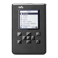
HAP-S1
93
Pin No. Pin Name I/O Description
V24, V25
DISP0_DAT22,
DISP0_DAT18
O RGB signal (red) output to the liquid crystal display
W1 LVDS0_TX3_P - Not used
W2 LVDS0_TX3_N - Not used
W3 GND93 - Ground terminal
W4 KEY_ROW2 - Not used
W5, W6
KEY_COL0,
KEY_COL2
- Not used
W7 to
W13
GND94 to GND100 - Ground terminal
W14 DRAM_A4 O Address signal output to the SD-RAM
W15 to
W19
GND101 to GND105 - Ground terminal
W20 ENET_TXD1 O
VBUS power on/off control signal output terminal for the WLAN/BT COMBO card
“H”: power on
W21 ENET_RXD0 - Not used
W22 ENET_RXD1 I Interrupt signal input from the ethernet transceiver
W23 ENET_RX_ER O ID signal output terminal for the USB OTG Not used
W24 DISP0_DAT23 O RGB signal (red) output to the liquid crystal display
W25 DRAM_D63 - Not used
Y1 LVDS1_TX0_N - Not used
Y2 LVDS1_TX0_P - Not used
Y3 LVDS1_CLK_N - Not used
Y4 LVDS1_CLK_P - Not used
Y5 GND106 - Ground terminal
Y6 DRAM_RESET O Reset signal output to the SD-RAM “L”: reset
Y7 to
Y10
DRAM_D20,
DRAM_D21,
DRAM_D19,
DRAM_D25
I/O Two-way data bus with the SD-RAM
Y11 DRAM_SDCKE0 O Clock enable signal output to the SD-RAM
Y12 to
Y14
DRAM_A15,
DRAM_A7,
DRAM_A3
O Address signal output to the SD-RAM
Y15 DRAM_SDBA1 O Bank address signal output to the SD-RAM
Y16 DRAM_CS0 O Chip select signal output to the SD-RAM
Y17 to
Y20
DRAM_D36,
DRAM_D37,
DRAM_D40,
DRAM_D44
- Not used
Y21 DRAM_DQM7 - Not used
Y22, Y23
DRAM_D59,
DRAM_D62
- Not used
Y24 GND107 - Ground terminal
Y25 DRAM_D58 - Not used
AA1 LVDS1_TX1_P - Not used
AA2 LVDS1_TX1_N - Not used
AA3 LVDS1_TX3_N - Not used
AA4 LVDS1_TX3_P - Not used
AA5,
AA6
DRAM_D3,
DRAM_D10
I/O Two-way data bus with the SD-RAM
AA7 GND10 - Ground terminal
AA8,
AA9
DRAM_D17,
DRAM_D23
I/O Two-way data bus with the SD-RAM
AA10 GND5 - Ground terminal
AA11 DRAM_SDCKE1 - Not used
AA12 DRAM_A14 O Address signal output to the SD-RAM
AA13 GND6 - Ground terminal
AA14,
AA15
DRAM_A2,
DRAM_A10
O Address signal output to the SD-RAM
AA16 GND7 - Ground terminal
AA17,
AA18
DRAM_D32,
DRAM_D33
- Not used
 Loading...


