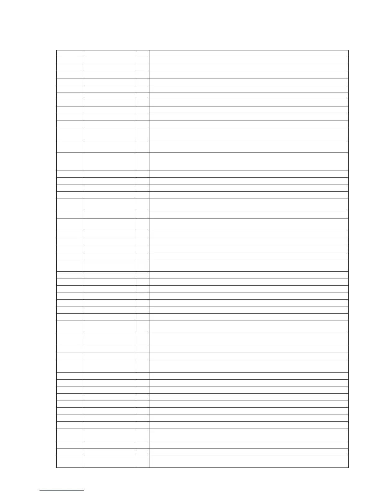
HAP-S1
97
Pin No. Pin Name I/O Description
A1 TDO O Data output terminal for the JTAG Not used
A2 TMS I Mode selection signal input terminal for the JTAG Not used
A3 TDI I Data input terminal for the JTAG Not used
A4 DCLK I Serial data transfer clock signal input from the MPU
A5 IO/DATA0 I Confi guration data input from the MPU
A6 IO/CLKUSR I Not used
A7 IO/PLL2_CLKOUTN O Not used
A8 IO/PLL2_CLKOUTP O Not used
A9 CLK8/DIFFCLK_5N I Audio data input from the audio DSP
A10 CLK9/DIFFCLK_5p I Not used
A11
IO/DIFFCLK_T11N/
DQ0T
O Bit clock signal output to the audio DSP
A12
IO/DIFFCLK_T11P/
DQ0T
O Not used
A13
IO/DIFFIO_T17N/
DQS0T/CQ0T/
DPCLK10
O Not used
B1, B2 GND_B1, GND_B2 - Ground terminal
B3 TCK I Clock signal input terminal for the JTAG Not used
B4 GND_B4 - Ground terminal
B5 IO/ASDO O Not used
B6
IO/DQS1T/CQ0T#/
DPCLK13
O Not used
B7 GND_B7 - Ground terminal
B8
IO/DIFFCLK_T12N/
DQ0T
O Bit clock signal output to the audio DSP
B9 GND_B9 - Ground terminal
B10 IO/VREFB7N0 O Audio data output to the audio DSP
B11 IO_B11 O L/R sampling clock signal output to the audio DSP
B12 GND_B12 - Ground terminal
B13
IO/DIFFIO_T17P/
DQ0T
O Not used
C1 GXB_TX1n O Not used
C2 GXB_TX1p O Not used
C3 VCCIO9_C3 - Power supply terminal (+3.3V)
C4 nCE I Chip enable signal input terminal Not used
C5 IO/NSCO O Not used
C6 IO/VREFB8N0 O Not used
C7 VCCIO8_C7 - Power supply terminal (+3.3V)
C8
IO/DIFFCLK_T12P/
DQ0T
O L/R sampling clock signal output to the audio DSP
C9, C10
VCCIO7_C9,
VCCIO7_C10
- Power supply terminal (+3.3V)
C11 IO/PUP4/DQ0T O Not used
C12 IO/PDN4/DQ0T O Not used
C13
IO/DiFFIO_T1BN/
DQ0T
O Not used
D1, D2 GND_D1, GND_D2 - Ground terminal
D3 VCCD_PLL_D3 - Power supply terminal (+1.2V)
D4 VCCA_D4 - Power supply terminal (+2.5V)
D5 nCONFIG I Confi guration signal input from the MPU
D6 GND_D6 - Ground terminal
D7 VCC_CLKIN8A - Power supply terminal (+2.5V)
D8 GND_D8 - Ground terminal
D9 VCCA_D9 - Power supply terminal (+2.5V)
D10
IO/DIFFIO_R4n/
DEV_CLRn
I Reset signal input from the MPU “L”: reset
D11 IO/DIFFIO_R2P O Chip select signal output to the D/A converter
D12 IO/DIFFIO_R2N O Serial data output to the D/A converter
D13
IO/DIFFIO_T1BP/
DQ0T
O Interrupt signal output to the MPU
FPGA DSP BOARD IC001 EP4CGX30BF14C8N (FPGA)
 Loading...