HAP-S1
96
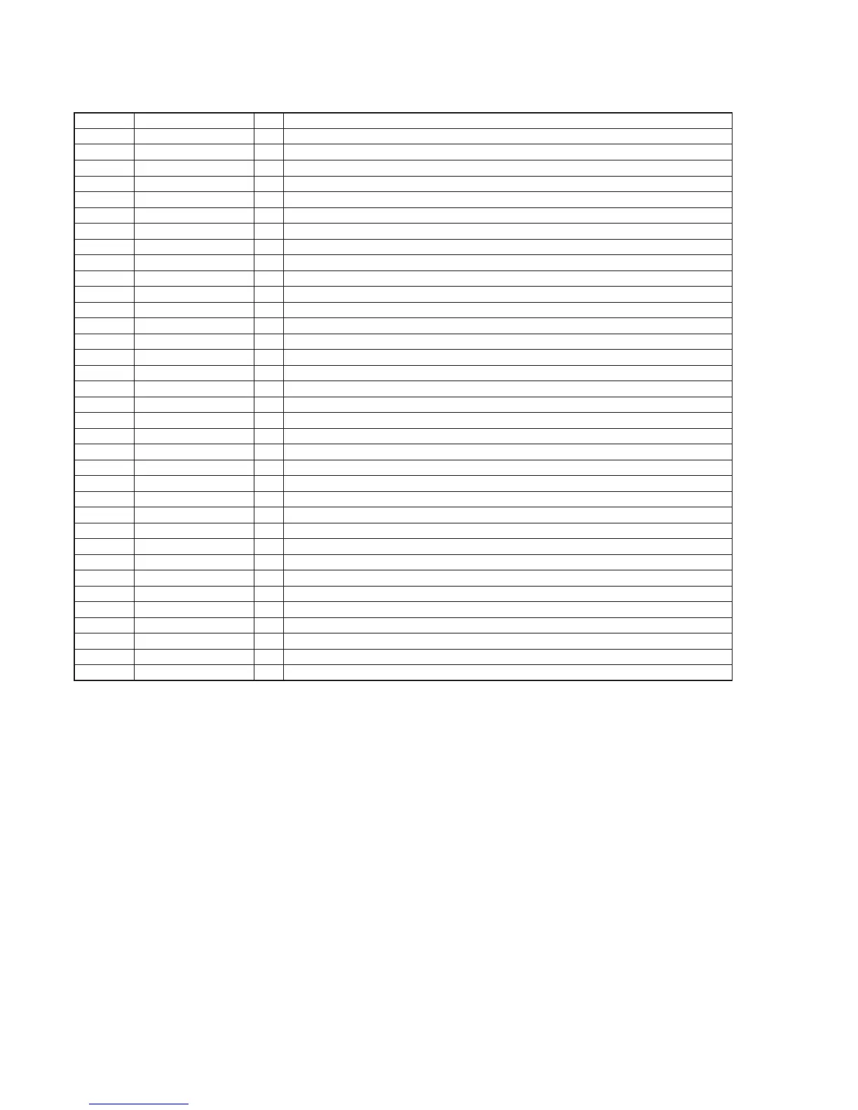
Pin No. Pin Name I/O Description
1 RSTN I Reset signal input from the MPU “L”: reset
2 LX O Internal regulator output terminal (+1.1V)
3 VDD33 - Power supply terminal (+3.3V)
4 XTALO O System clock output terminal (25 MHz)
5 XTALI I System clock input terminal (25 MHz)
6 AVDDL_6 - Power supply terminal (+1.1V)
7 RBIAS O Bias current setting terminal
8 VDDH_REG O Internal regulator output terminal (+2.5V)
9 TRXP0 I/O Two-way data (positive) bus with the LAN jack
10 TRXN0 I/O Two-way data (negative) bus with the LAN jack
11 AVDDL_11 - Power supply terminal (+1.1V)
12 TRXP1 I/O Two-way data (positive) bus with the LAN jack
13 TRXN1 I/O Two-way data (negative) bus with the LAN jack
14 AVDD33 - Power supply terminal (+3.3V)
15 TRXP2 I/O Two-way data (positive) bus with the LAN jack
16 TRXN2 I/O Two-way data (negative) bus with the LAN jack
17 AVDDL_17 - Power supply terminal (+1.1V)
18 TRXP3 I/O Two-way data (positive) bus with the LAN jack
19 TRXN3 I/O Two-way data (negative) bus with the LAN jack
20 INT O Interrupt signal output to the MPU
21 LED_ACT O LED drive signal output terminal Not used
22 LED_1000 O LED drive signal output terminal Not used
23 CLK_25M O 25 MHz clock signal output to the MPU
24 LED_10_100 O LED drive signal output terminal Not used
25, 26 RXD3, RXD2 O RGMII receive data output to the MPU
27 VDDIO_REG O Internal regulator output terminal (+1.8V)
28, 29 RXD1, RXD0 O RGMII receive data output to the MPU
30 RX_DV O RGMII receive data valid signal output to the MPU
31 RX_CLK O RGMII receive clock signal output to the MPU
32 TX_EN I RGMII transmit data enable signal input from the MPU
33 GTX_CLK I RGMII transmit clock signal input from the MPU
34 to 37 TXD0 toTXD3 I RGMII transmit data input from the MPU
38 DVDDL - Power supply terminal (+1.1V)
39 MDIO I/O Two-way management data bus with the MPU
40 MDC I Management data clock signal input from the MPU
MAIN BOARD IC602 AR8035-AL1A (ETHERNET TRANSCEIVER, +1.1V/+1.8V REGULATOR)
 Loading...