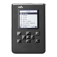
HAP-S1
95
Pin No. Pin Name I/O Description
AD7 GND19 - Ground terminal
AD8 DRAM_SDQS2 O Data strobe signal (upper byte) output to the SD-RAM
AD9 DRAM_D29 I/O Two-way data bus with the SD-RAM
AD10 GND13 - Ground terminal
AD11 DRAM_D30 I/O Two-way data bus with the SD-RAM
AD12 DRAM_A12 O Address signal output to the SD-RAM
AD13 GND14 - Ground terminal
AD14 DRAM_SDCLK_1 O Clock signal output to the SD-RAM
AD15 DRAM_SDCLK_0 - Not used
AD16 GND15 - Ground terminal
AD17 DRAM_CS1 - Not used
AD18 DRAM_SDQS4 - Not used
AD19 GND16 - Ground terminal
AD20 DRAM_SDQS5 - Not used
AD21 DRAM_D43 - Not used
AD22 GND17 - Ground terminal
AD23 DRAM_SDQS6 - Not used
AD24 DRAM_DQM6 - Not used
AD25 DRAM_D54 - Not used
AE1 GND20 - Ground terminal
AE2 DRAM_D1 I/O Two-way data bus with the SD-RAM
AE3 DRAM_SDQS0 O Data strobe signal (lower byte) output to the SD-RAM
AE4,
AE5
DRAM_D7,
DRAM_D9
I/O Two-way data bus with the SD-RAM
AE6 DRAM_SDQS1_B O Data strobe signal (upper byte) output to the SD-RAM
AE7 DRAM_D11 I/O Two-way data bus with the SD-RAM
AE8 DRAM_SDQS2_B O Data strobe signal (upper byte) output to the SD-RAM
AE9 DRAM_D24 I/O Two-way data bus with the SD-RAM
AE10 DRAM_DQM3 O Data mask (lower byte) signal output to the SD-RAM
AE11 DRAM_D26 I/O Two-way data bus with the SD-RAM
AE12,
AE13
DRAM_A9,
DRAM_A5
O Address signal output to the SD-RAM
AE14 DRAM_SDCLK_1_B O Clock signal output to the SD-RAM
AE15 DRAM_SDCLK_0_B - Not used
AE16 DRAM_CAS O Column address signal output to the SD-RAM
AE17 ZQPAD I External calibration resistor connection terminal
AE18 DRAM_SDQS4_B - Not used
AE19 DRAM_D35 - Not used
AE20 DRAM_SDQS5_B - Not used
AE21,
AE22
DRAM_D46,
DRAM_D49
- Not used
AE23 DRAM_SDQS6_B - Not used
AE24 DRAM_D50 - Not used
AE25 GND21 - Ground terminal
 Loading...