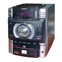
HCD-GT3D
68
Pin No. Pin Name I/O Description
107 Vss - Ground terminal
108
TEST-MON108/
SD_CLK
O Test port for software checking
109 PVcc - Power supply terminal (+3.3V)
110
TEST-MON110/
SD_D0_0
O Test port for software checking
111
ANALOG-DSEL/
SD_D1_0
O ANALOG INPUT SELECTOR D
112
RGB-TRANS-LED-
SPK/SD_WP_0
O Transfer signal to RGB driver (driver for Speaker LED)
113
RGB-TRANS-LED/
SD_CD_0
O Transfer signal to RGB driver
114 ST-RDS I Input for RDS Text Detect Signal (L: RDS Detect)
115 ST-CE O Tuner IC: Tuner enable input pin
116 Vss - Ground terminal
117 PCONT-DAMP O Digital Amp Module Power Control Pin. “H”: ON
118 RGB-PWM-CLK O PWM clock signal to RGB driver
119 Vcc - Power supply terminal (+3.3V)
120 /AMP-RESET O Digital Amp Reset Pin
121 Vss - Ground terminal
122 CD-MOTOR+ O CDM turning motor control signal output
123 PVcc - Power supply terminal (+3.3V)
124 CD-MOTOR- O CDM turning motor control signal output
125 DIR_CP-CLK O DIR & CP share clock
126 DIR_CP-DATA I/O DIR & CP share data
127 ST-CLK O Tuner IC: Clock signal for IIC communication
128 ST-DATA I/O Tuner IC: Data signal for IIC communication
129 RELAY CONTROL O Relay control
130 DIR INT0 I DIR INTERRUPT 0
131 NFC_CLK O NFC CLOCK
132 NFC_DATA I/O Two-way data bus with the NFC
133 BT-TxD O TX signal output terminal for Bluetooth section
134 LCD_INHB O FL inhibit pin
135 SIRCS I Remote control signal input
136 DIR INT1 I DIR INTERRUPT 1
137 RGB-SCLK O Serial clock output to RGB driver
138 Vss - Ground terminal
139 USB_X1 I USB clock input terminal
140 USB_X2 O USB clock output terminal
141 USBDPVcc - Power supply terminal (+3.3V)
142 USBDPVss - Ground terminal
143 DM1 - Not used
144 DP1 - Not used
145 VBUSIN1 - Not used
146 USBDVcc - Power supply terminal (+3.3V)
147 USBDVss - Ground terminal
148 USBDPVcc - Power supply terminal (+3.3V)
149 USBDPVss - Ground terminal
150 USB_DM0 I/O D- PIN FOR USB 2.0
151 USB_DP0 I/O D+ PIN FOR USB 2.0
152 VBUSIN0 O VBUS +5.0V supply monitoring pin
153 USBDVcc - Power supply terminal (+3.3V)
154 USBDVss - Ground terminal
155 REFRIN I Reference input
156 USBAPVss - Ground terminal
157 USBAPVcc - Power supply terminal (+3.3V)
158 USBAVcc - Power supply terminal (+3.3V)
 Loading...