t
w(RSL)
t
h(XPLLDIS)
t
OSCST
V , V
V , V
(3.3 V)
DDIO DD3VFL
DDAn DDAIO
XCLKIN
X1
XRS
XF/XPLLDIS
XMP/MC
V , V
[1.8 V (or 1.9 V)]
DD DD1
I/O Pins
XPLLDIS Sampling
Address/
Data/
Control
XCLKOUT
Input Configuration (State Depends on Internal PU/PD)
Address/Data/Control Valid Execution
Begins From External Boot Address 0x3FFFC0
XCLKIN/8
(A)
User-Code Dependent
2.5 V
0.3 V
(Don’t Care)
t
d(EX)
t
h(XMP/MC)
(Don’t Care)
(B)
User-Code Dependent
(Don’t Care)
GPIOF14/XF (User-Code Dependent)
t
su(XPLLDIS)
TMS320F2810, TMS320F2811, TMS320F2812
TMS320C2810, TMS320C2811, TMS320C2812
SPRS174T –APRIL 2001–REVISED MAY 2012
www.ti.com
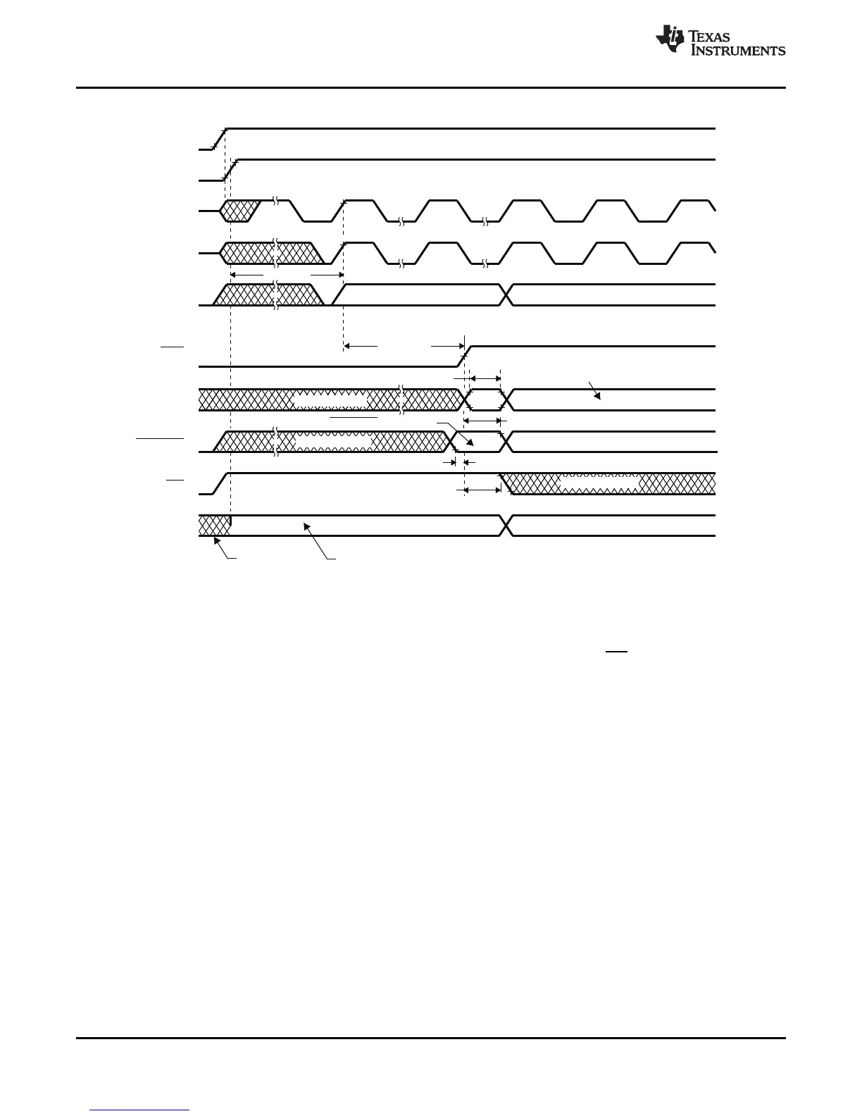
A. Upon power up, SYSCLKOUT is XCLKIN/2 if the PLL is enabled. Since both the XTIMCLK and CLKMODE bits in the
XINTCNF2 register come up with a reset state of 1, SYSCLKOUT is further divided by 4 before it appears at
XCLKOUT. This explains why XCLKOUT = XCLKIN/8 during this phase.
B. The state of the GPIO pins is undefined (that is, they could be input or output) until the 1.8-V (or 1.9-V) supply
reaches at least 1 V and 3.3-V supply reaches 2.5 V.
Figure 6-12. Power-on Reset in Microprocessor Mode (XMP/MC = 1)
106 Electrical Specifications Copyright © 2001–2012, Texas Instruments Incorporated
Submit Documentation Feedback
Product Folder Link(s): TMS320F2810 TMS320F2811 TMS320F2812 TMS320C2810 TMS320C2811 TMS320C2812