INT[12:1]
CLKIN
Real-Time JTAG
Peripheral Bus
C28x CPU
INT14
NMI
INT13
Memory Bus
Flash
128K x 16 (F2812)
128K x 16 (F2811)
64K x 16 (F2810)
eCAN
SCIA/SCIB
12-Bit ADC
External Interrupt
Control
(XINT1/2/13, XNMI)
EVA/EVB
Memory Bus
OTP
1K x 16
(C)
McBSP
System Control
(Oscillator and PLL
+
Peripheral Clocking
+
Low-Power Modes
+
Watchdog)
FIFO
FIFO
PIE
(96 Interrupts)
(A)
RS
SPI
FIFO
TINT0
TINT1
TINT2
CPU-Timer 0
CPU-Timer 1
CPU-Timer 2
16 Channels
GPIO Pins
XRS
X1/XCLKIN
X2
XF_XPLLDIS
Protected by the code-security module.
XINT13
G
P
I
O
M
U
X
XNMI
ROM
128K x 16 (C2812)
128K x 16 (C2811)
64K x 16 (C2810)
Control
Address (19)
Data (16)
External
Interface
(XINTF)
(B)
L0 SARAM
4K x 16
L1 SARAM
4K x 16
M1 SARAM
1K x 16
M0 SARAM
1K x 16
H0 SARAM
8K x 16
Boot ROM
4K x 16
TMS320F2810, TMS320F2811, TMS320F2812
TMS320C2810, TMS320C2811, TMS320C2812
SPRS174T –APRIL 2001–REVISED MAY 2012
www.ti.com
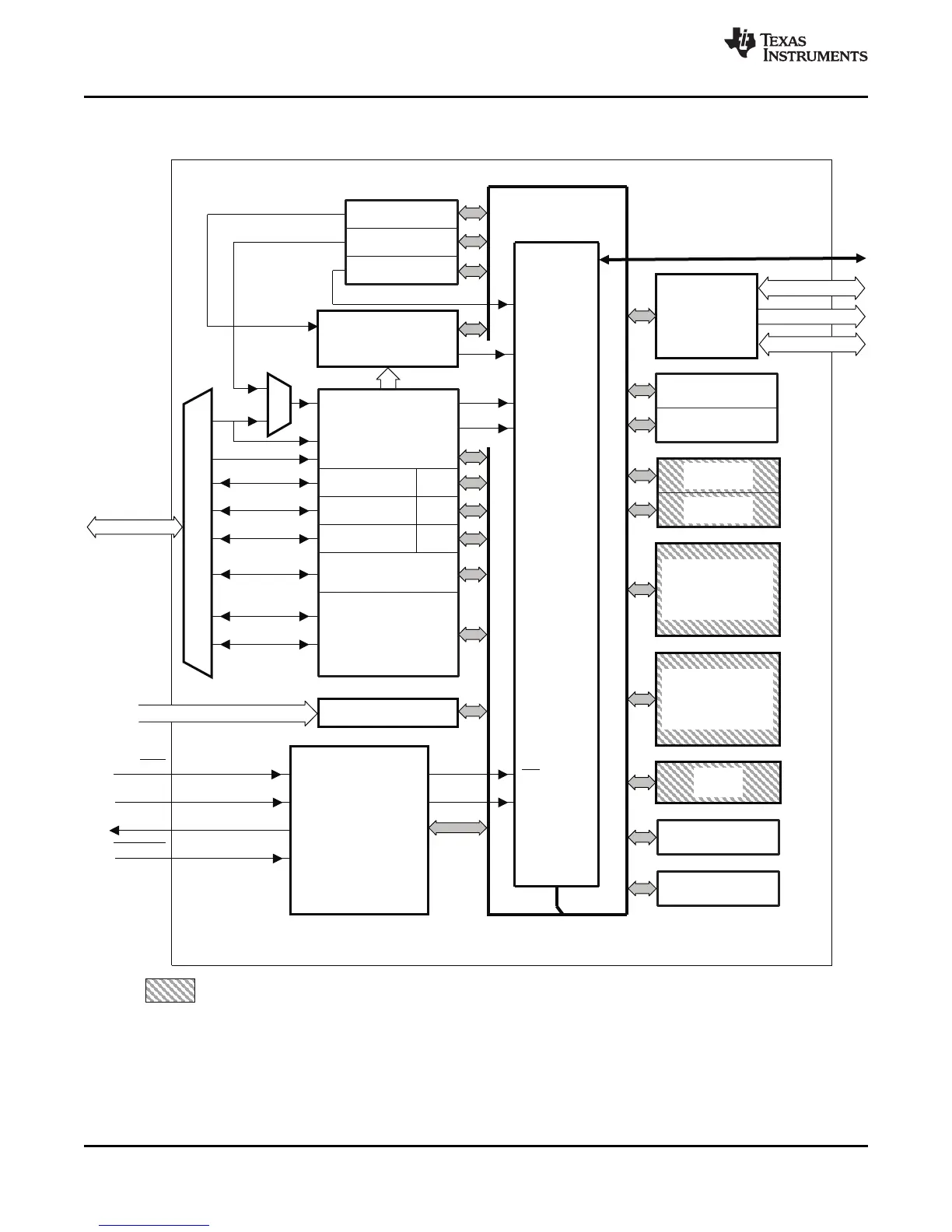
3 Functional Overview
A. 45 of the possible 96 interrupts are used on the devices.
B. XINTF is available on the F2812 and C2812 devices only.
C. On C281x devices, the OTP is replaced with a 1K x 16 block of ROM.
Figure 3-1. Functional Block Diagram
26 Functional Overview Copyright © 2001–2012, Texas Instruments Incorporated
Submit Documentation Feedback
Product Folder Link(s): TMS320F2810 TMS320F2811 TMS320F2812 TMS320C2810 TMS320C2811 TMS320C2812