INT1
to
INT12
INT14
C28x
CPU
TINT2
TINT0
PIE
CPU-TIMER 2
(Reserved for
DSP/BIOS)
INT13
TINT1
XINT13
CPU-TIMER 0
CPU-TIMER 1
TMS320F2810, TMS320F2811, TMS320F2812
TMS320C2810, TMS320C2811, TMS320C2812
SPRS174T –APRIL 2001–REVISED MAY 2012
www.ti.com
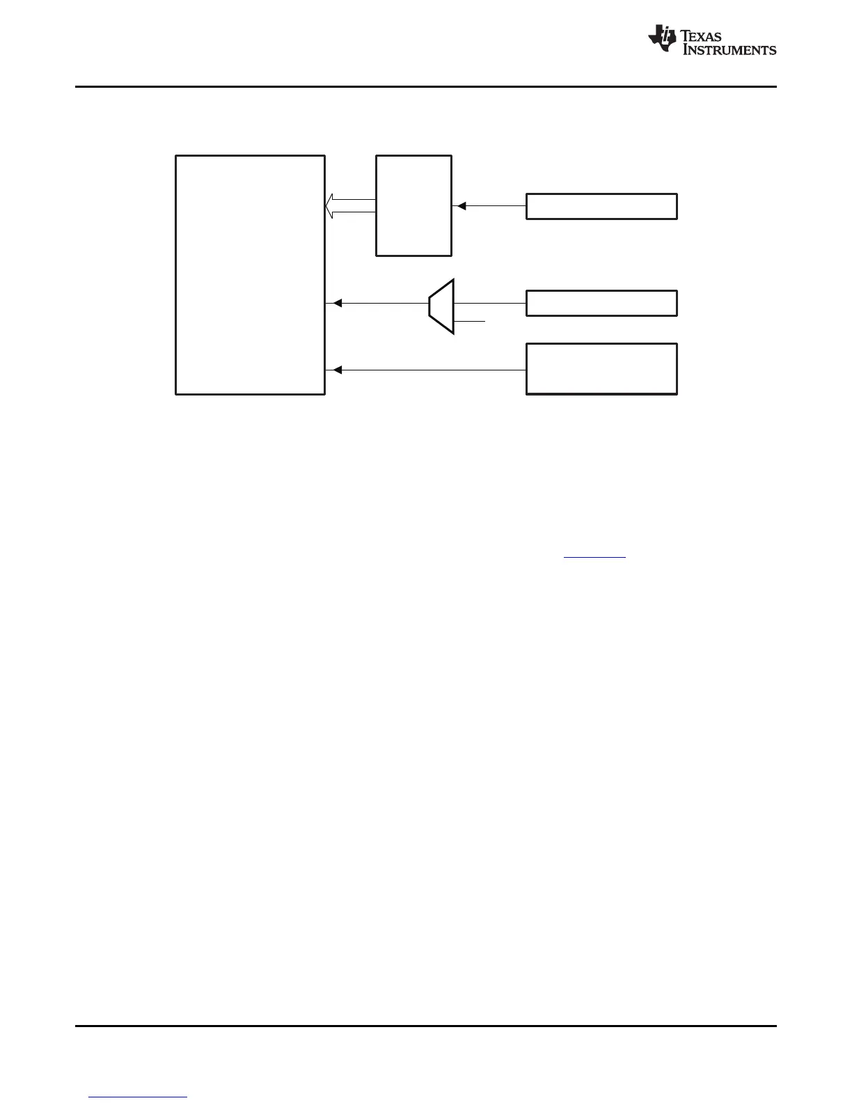
In the F281x and C281x devices, the timer interrupt signals (TINT0, TINT1, TINT2) are connected as
shown in Figure 4-2.
A. The timer registers are connected to the memory bus of the C28x processor.
B. The timing of the timers is synchronized to SYSCLKOUT of the processor clock.
Figure 4-2. CPU-Timer Interrupts Signals and Output Signal
The general operation of the timer is as follows: The 32-bit counter register “TIMH:TIM” is loaded with the
value in the period register “PRDH:PRD”. The counter register decrements at the SYSCLKOUT rate of the
C28x. When the counter reaches 0, a timer interrupt output signal generates an interrupt pulse. The
registers listed in Table 4-1 are used to configure the timers. For more information, see the TMS320x281x
DSP System Control and Interrupts Reference Guide (literature number SPRU078).
56 Peripherals Copyright © 2001–2012, Texas Instruments Incorporated
Submit Documentation Feedback
Product Folder Link(s): TMS320F2810 TMS320F2811 TMS320F2812 TMS320C2810 TMS320C2811 TMS320C2812