TMS320F2810, TMS320F2811, TMS320F2812
TMS320C2810, TMS320C2811, TMS320C2812
www.ti.com
SPRS174T –APRIL 2001–REVISED MAY 2012
2.4 Signal Descriptions
Table 2-2 specifies the signals on the F281x and C281x devices. All digital inputs are TTL-compatible. All
outputs are 3.3 V with CMOS levels. Inputs are not 5-V tolerant. A 100-µA (or 20-µA) pullup/pulldown is
used.
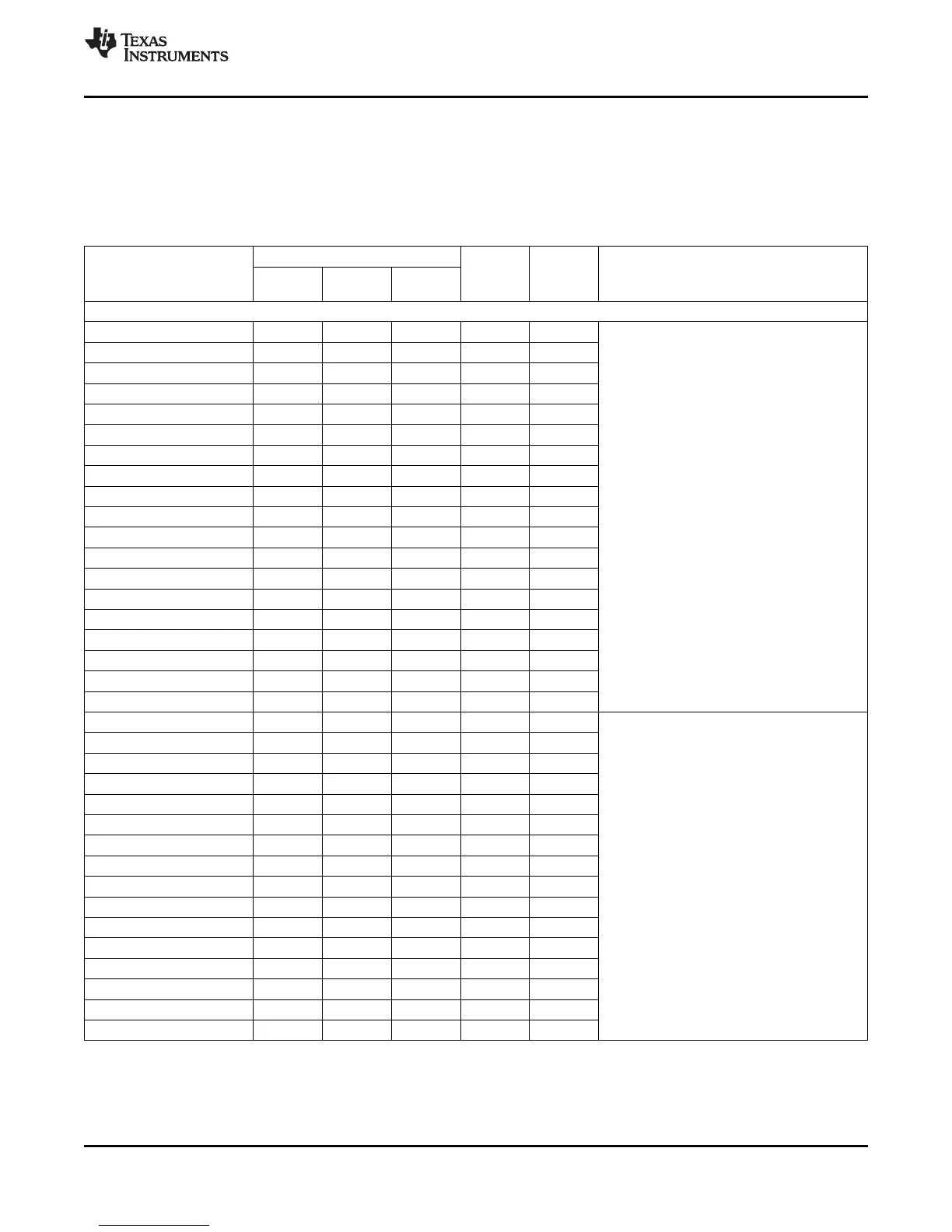
Table 2-2. Signal Descriptions
(1)
PIN NO.
NAME I/O/Z
(2)
PU/PD
(3)
DESCRIPTION
179-BALL 176-PIN 128-PIN
GHH/ZHH PGF PBK
XINTF SIGNALS (2812 ONLY)
XA[18] D7 158 – O/Z –
XA[17] B7 156 – O/Z –
XA[16] A8 152 – O/Z –
XA[15] B9 148 – O/Z –
XA[14] A10 144 – O/Z –
XA[13] E10 141 – O/Z –
XA[12] C11 138 – O/Z –
XA[11] A14 132 – O/Z –
XA[10] C12 130 – O/Z –
XA[9] D14 125 – O/Z – 19-bit XINTF Address Bus
XA[8] E12 121 – O/Z –
XA[7] F12 118 – O/Z –
XA[6] G14 111 – O/Z –
XA[5] H13 108 – O/Z –
XA[4] J12 103 – O/Z –
XA[3] M11 85 – O/Z –
XA[2] N10 80 – O/Z –
XA[1] M2 43 – O/Z –
XA[0] G5 18 – O/Z –
XD[15] A9 147 – I/O/Z PU
XD[14] B11 139 – I/O/Z PU
XD[13] J10 97 – I/O/Z PU
XD[12] L14 96 – I/O/Z PU
XD[11] N9 74 – I/O/Z PU
XD[10] L9 73 – I/O/Z PU
XD[9] M8 68 – I/O/Z PU
XD[8] P7 65 – I/O/Z PU
16-bit XINTF Data Bus
XD[7] L5 54 – I/O/Z PU
XD[6] L3 39 – I/O/Z PU
XD[5] J5 36 – I/O/Z PU
XD[4] K3 33 – I/O/Z PU
XD[3] J3 30 – I/O/Z PU
XD[2] H5 27 – I/O/Z PU
XD[1] H3 24 – I/O/Z PU
XD[0] G3 21 – I/O/Z PU
(1) Typical drive strength of the output buffer for all pins is 4 mA except for TDO, XCLKOUT, XF, XINTF, EMU0, and EMU1 pins, which are
8 mA.
(2) I = Input, O = Output, Z = High impedance
(3) PU = pin has internal pullup; PD = pin has internal pulldown. Pullup/pulldown strength is given in Section 6.3, Electrical Characteristics
Over Recommended Operating Conditions. The pullups/pulldowns are enabled in boundary scan mode.
Copyright © 2001–2012, Texas Instruments Incorporated Introduction 17
Submit Documentation Feedback
Product Folder Link(s): TMS320F2810 TMS320F2811 TMS320F2812 TMS320C2810 TMS320C2811 TMS320C2812