TMS320F2810, TMS320F2811, TMS320F2812
TMS320C2810, TMS320C2811, TMS320C2812
www.ti.com
SPRS174T –APRIL 2001–REVISED MAY 2012
4.8 GPIO MUX
The GPIO Mux registers are used to select the operation of shared pins on the F281x and C281x devices.
The pins can be individually selected to operate as “Digital I/O” or connected to “Peripheral I/O” signals
(via the GPxMUX registers). If selected for “Digital I/O”mode, registers are provided to configure the pin
direction (via the GPxDIR registers) and to qualify the input signal to remove unwanted noise (via the
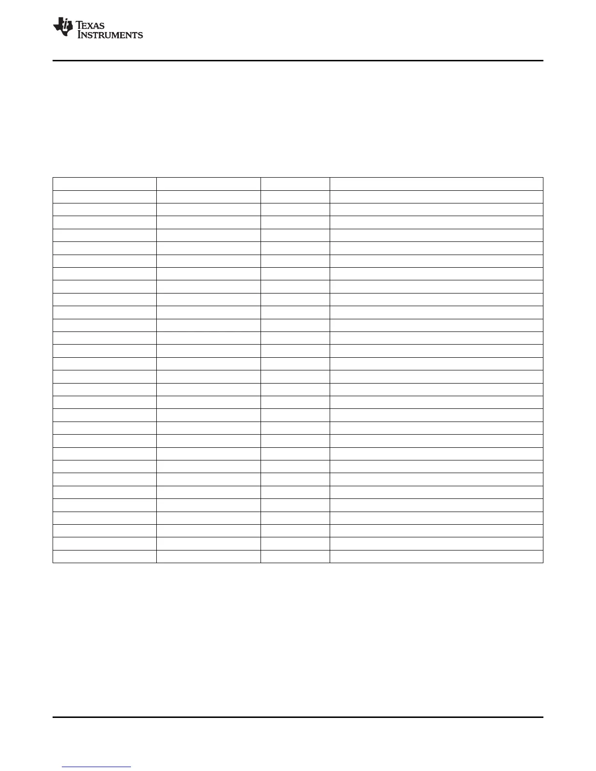
GPxQUAL) registers). Table 4-11 lists the GPIO Mux Registers.
Table 4-11. GPIO Mux Registers
(1)(2)(3)
NAME ADDRESS SIZE (x16) DESCRIPTION
GPAMUX 0x00 70C0 1 GPIO A Mux Control Register
GPADIR 0x00 70C1 1 GPIO A Direction Control Register
GPAQUAL 0x00 70C2 1 GPIO A Input Qualification Control Register
Reserved 0x00 70C3 1
GPBMUX 0x00 70C4 1 GPIO B Mux Control Register
GPBDIR 0x00 70C5 1 GPIO B Direction Control Register
GPBQUAL 0x00 70C6 1 GPIO B Input Qualification Control Register
Reserved 0x00 70C7 1
Reserved 0x00 70C8 1
Reserved 0x00 70C9 1
Reserved 0x00 70CA 1
Reserved 0x00 70CB 1
GPDMUX 0x00 70CC 1 GPIO D Mux Control Register
GPDDIR 0x00 70CD 1 GPIO D Direction Control Register
GPDQUAL 0x00 70CE 1 GPIO D Input Qualification Control Register
Reserved 0x00 70CF 1
GPEMUX 0x00 70D0 1 GPIO E Mux Control Register
GPEDIR 0x00 70D1 1 GPIO E Direction Control Register
GPEQUAL 0x00 70D2 1 GPIO E Input Qualification Control Register
Reserved 0x00 70D3 1
GPFMUX 0x00 70D4 1 GPIO F Mux Control Register
GPFDIR 0x00 70D5 1 GPIO F Direction Control Register
Reserved 0x00 70D6 1
Reserved 0x00 70D7 1
GPGMUX 0x00 70D8 1 GPIO G Mux Control Register
GPGDIR 0x00 70D9 1 GPIO G Direction Control Register
Reserved 0x00 70DA 1
Reserved 0x00 70DB 1
Reserved 0x00 70DC – 0x00 70DF 4
(1) Reserved locations return undefined values and writes are ignored.
(2) Not all inputs support input signal qualification.
(3) These registers are EALLOW protected. This prevents spurious writes from overwriting the contents and corrupting the system.
Copyright © 2001–2012, Texas Instruments Incorporated Peripherals 83
Submit Documentation Feedback
Product Folder Link(s): TMS320F2810 TMS320F2811 TMS320F2812 TMS320C2810 TMS320C2811 TMS320C2812