TMS320F2810, TMS320F2811, TMS320F2812
TMS320C2810, TMS320C2811, TMS320C2812
www.ti.com
SPRS174T –APRIL 2001–REVISED MAY 2012
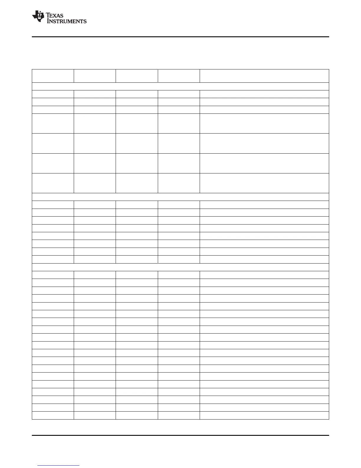
Table 4-7 provides a summary of the McBSP registers.
Table 4-7. McBSP Registers
ADDRESS TYPE RESET VALUE
NAME DESCRIPTION
0x00 78xxh (R/W) (HEX)
DATA REGISTERS, RECEIVE, TRANSMIT
(1)
– – – 0x0000 McBSP Receive Buffer Register
– – – 0x0000 McBSP Receive Shift Register
– – – 0x0000 McBSP Transmit Shift Register
McBSP Data Receive Register 2
DRR2 00 R 0x0000
• Read First if the word size is greater than 16 bits,
else ignore DRR2
McBSP Data Receive Register 1
DRR1 01 R 0x0000
• Read Second if the word size is greater than 16 bits,
else read DRR1 only
McBSP Data Transmit Register 2
DXR2 02 W 0x0000
• Write First if the word size is greater than 16 bits,
else ignore DXR2
McBSP Data Transmit Register 1
DXR1 03 W 0x0000
• Write Second if the word size is greater than 16 bits,
else write to DXR1 only
McBSP CONTROL REGISTERS
SPCR2 04 R/W 0x0000 McBSP Serial Port Control Register 2
SPCR1 05 R/W 0x0000 McBSP Serial Port Control Register 1
RCR2 06 R/W 0x0000 McBSP Receive Control Register 2
RCR1 07 R/W 0x0000 McBSP Receive Control Register 1
XCR2 08 R/W 0x0000 McBSP Transmit Control Register 2
XCR1 09 R/W 0x0000 McBSP Transmit Control Register 1
SRGR2 0A R/W 0x0000 McBSP Sample Rate Generator Register 2
SRGR1 0B R/W 0x0000 McBSP Sample Rate Generator Register 1
MULTICHANNEL CONTROL REGISTERS
MCR2 0C R/W 0x0000 McBSP Multichannel Register 2
MCR1 0D R/W 0x0000 McBSP Multichannel Register 1
RCERA 0E R/W 0x0000 McBSP Receive Channel Enable Register Partition A
RCERB 0F R/W 0x0000 McBSP Receive Channel Enable Register Partition B
XCERA 10 R/W 0x0000 McBSP Transmit Channel Enable Register Partition A
XCERB 11 R/W 0x0000 McBSP Transmit Channel Enable Register Partition B
PCR 12 R/W 0x0000 McBSP Pin Control Register
RCERC 13 R/W 0x0000 McBSP Receive Channel Enable Register Partition C
RCERD 14 R/W 0x0000 McBSP Receive Channel Enable Register Partition D
XCERC 15 R/W 0x0000 McBSP Transmit Channel Enable Register Partition C
XCERD 16 R/W 0x0000 McBSP Transmit Channel Enable Register Partition D
RCERE 17 R/W 0x0000 McBSP Receive Channel Enable Register Partition E
RCERF 18 R/W 0x0000 McBSP Receive Channel Enable Register Partition F
XCERE 19 R/W 0x0000 McBSP Transmit Channel Enable Register Partition E
XCERF 1A R/W 0x0000 McBSP Transmit Channel Enable Register Partition F
RCERG 1B R/W 0x0000 McBSP Receive Channel Enable Register Partition G
RCERH 1C R/W 0x0000 McBSP Receive Channel Enable Register Partition H
XCERG 1D R/W 0x0000 McBSP Transmit Channel Enable Register Partition G
XCERH 1E R/W 0x0000 McBSP Transmit Channel Enable Register Partition H
(1) DRR2/DRR1 and DXR2/DXR1 share the same addresses of receive and transmit FIFO registers in FIFO mode.
Copyright © 2001–2012, Texas Instruments Incorporated Peripherals 75
Submit Documentation Feedback
Product Folder Link(s): TMS320F2810 TMS320F2811 TMS320F2812 TMS320C2810 TMS320C2811 TMS320C2812