TMS320F2810, TMS320F2811, TMS320F2812
TMS320C2810, TMS320C2811, TMS320C2812
www.ti.com
SPRS174T –APRIL 2001–REVISED MAY 2012
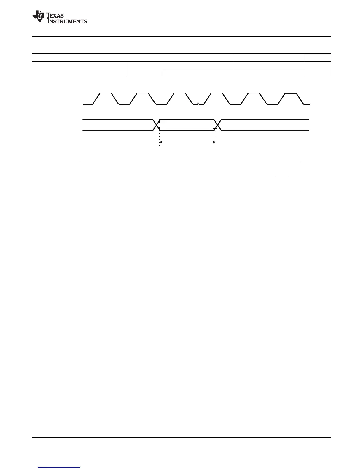
Table 6-25. General-Purpose Input Timing Requirements
MIN MAX UNIT
With no qualifier 2t
c(SCO)
Pulse duration GPIO
t
w(GPI)
All GPIOs cycles
low/high
With qualifier 1t
c(SCO)
+ IQT
(1)
(1) Input Qualification Time (IQT) = [t
c(SCO)
× 2 × QUALPRD] × 5 + [t
c(SCO)
× 2 × QUALPRD].
Figure 6-25. General-Purpose Input Timing
NOTE
The pulse width requirement for general-purpose input is applicable for the XBIO and
ADCSOC pins as well.
6.20 Serial Peripheral Interface (SPI) Master Mode Timing
Table 6-26 lists the master mode timing (clock phase = 0) and Table 6-27 lists the timing (clock
phase = 1). Figure 6-26 and Figure 6-27 show the timing waveforms.
Copyright © 2001–2012, Texas Instruments Incorporated Electrical Specifications 117
Submit Documentation Feedback
Product Folder Link(s): TMS320F2810 TMS320F2811 TMS320F2812 TMS320C2810 TMS320C2811 TMS320C2812