TMS320F2810, TMS320F2811, TMS320F2812
TMS320C2810, TMS320C2811, TMS320C2812
www.ti.com
SPRS174T –APRIL 2001–REVISED MAY 2012
6.24 External Interface Read Timing
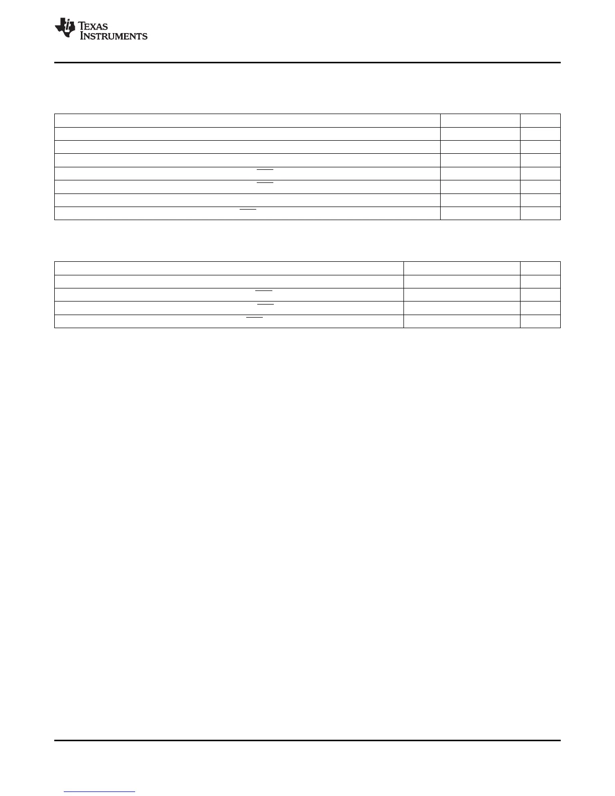
Table 6-32. External Memory Interface Read Switching Characteristics
PARAMETER MIN MAX UNIT
t
d(XCOH-XZCSL)
Delay time, XCLKOUT high to zone chip-select active-low 1 ns
t
d(XCOHL-XZCSH)
Delay time, XCLKOUT high/low to zone chip-select inactive-high –2 3 ns
t
d(XCOH-XA)
Delay time, XCLKOUT high to address valid 2 ns
t
d(XCOHL-XRDL)
Delay time, XCLKOUT high/low to XRD active-low 1 ns
t
d(XCOHL-XRDH)
Delay time, XCLKOUT high/low to XRD inactive-high –2 1 ns
t
h(XA)XZCSH
Hold time, address valid after zone chip-select inactive-high
(1)
ns
t
h(XA)XRD
Hold time, address valid after XRD inactive-high
(1)
ns
(1) During inactive cycles, the XINTF address bus will always hold the last address put out on the bus. This includes alignment cycles.
Table 6-33. External Memory Interface Read Timing Requirements
MIN MAX UNIT
t
a(A)
Access time, read data from address valid (LR + AR) – 14
(1)
ns
t
a(XRD)
Access time, read data valid from XRD active-low AR – 12
(1)
ns
t
su(XD)XRD
Setup time, read data valid before XRD strobe inactive-high 12 ns
t
h(XD)XRD
Hold time, read data valid after XRD inactive-high 0 ns
(1) LR = Lead period, read access. AR = Active period, read access. See Table 6-30.
Copyright © 2001–2012, Texas Instruments Incorporated Electrical Specifications 131
Submit Documentation Feedback
Product Folder Link(s): TMS320F2810 TMS320F2811 TMS320F2812 TMS320C2810 TMS320C2811 TMS320C2812